A fixing device used for silicon corrsion
A technology of fixing devices and snapping devices, applied in the field of computers, can solve problems such as low pass rate, poor quality of silicon wafers, large contact area between silicon chips and accommodating devices, etc., and achieve the goal of improving quality and pass rate, and reducing contact area Effect
- Summary
- Abstract
- Description
- Claims
- Application Information
AI Technical Summary
Problems solved by technology
Method used
Image

Examples
Embodiment 1
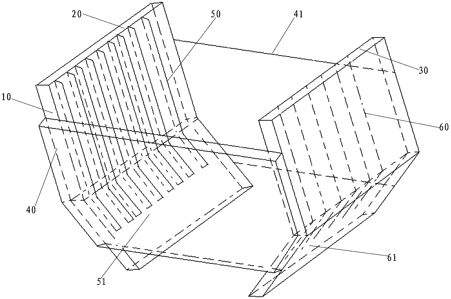
[0046] see figure 1 , the embodiment of the present application provides a fixing device applied to silicon etching, the fixing device 10 includes a first rack 20 and a second rack 30 and a connecting device for connecting the first rack 20 and the second rack 30 , the connecting device includes a first connecting piece 40 and a second connecting piece 41 .
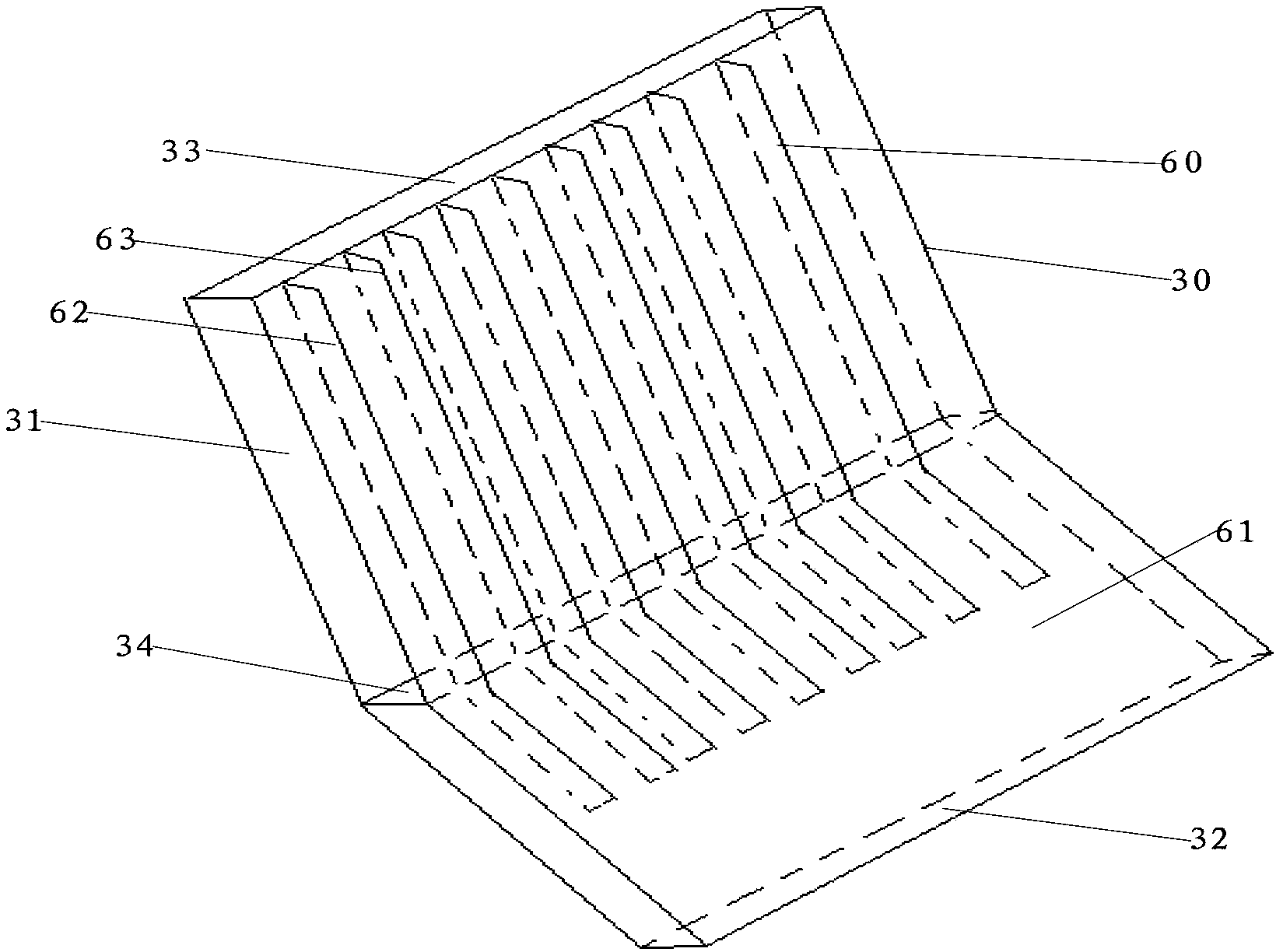
[0047] Wherein, the first engaging device 50 is fixedly connected to the inner side of the first sheet frame 20, the second engaging device 60 is fixedly connected to the inner side of the second sheet frame 30, and the lower end of the first engaging device 50 has a first concave portion 51, The lower end of the second engaging device 60 has a second concave portion 61 .
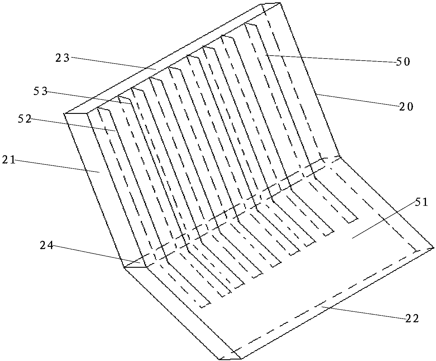
[0048] see figure 2 The first rack 20 includes a first frame 21, a first bottom column 22 fixed on the lower end of the first frame 21 and a first upper column 23 fixed on the top of the first frame 21, and the middle part of the first frame 21 is f...
Embodiment 2
[0063] Embodiment 2 of the present application differs from Embodiment 1 in that the structures of the first engaging device and the second engaging device are different. For the sake of brevity in the description, for the similarities between Embodiment 2 and Embodiment 1 of the present application, reference may be made to Example 1, which will not be repeated here. The difference between the second embodiment of the present application and the first implementation is described in detail below, specifically including:
[0064] The first engaging device 50 includes N clips, wherein N is an integer not less than 2, that is, the first engaging device includes at least a first clip and a second clip. see Figure 9 , taking the first engaging device 50 only including the first clamping piece 52 and the second clamping piece 53 as an example. The first clip 52 includes a first connecting piece 54 and a fifth connecting piece 58. The fifth connecting piece 58 is fixed on the lowe...
Embodiment 3
[0074] The difference between Embodiment 3 of the present application and Embodiment 1 is that a first supporting device is fixedly connected to the outer side of the first rack, and a second supporting device is fixedly connected to the outer side of the second rack, so that the fixing device Remains stable during silicon wafer etching. For the brevity of the description, for the similarities between Embodiment 3 and Embodiment 1 of the present application, reference may be made to Example 1, which will not be repeated here. The difference between Embodiment 3 of the present application and Implementation 1 is described in detail below, specifically including:
[0075] The first supporting device includes N clips, wherein N is an integer not less than 2, that is, the first supporting device includes at least a fifth clip and a sixth clip. see Figure 11 , taking the first supporting device including the fifth clamping piece and the sixth clamping piece as an example. A fir...
PUM
 Abstract
Description
Claims
Application Information
 - Generate Ideas
- Intellectual Property
- Life Sciences
- Materials
- Tech Scout
- Unparalleled Data Quality
- Higher Quality Content
- 60% Fewer Hallucinations
Browse by: Latest US Patents, China's latest patents, Technical Efficacy Thesaurus, Application Domain, Technology Topic, Popular Technical Reports.
© 2025 PatSnap. All rights reserved.Legal|Privacy policy|Modern Slavery Act Transparency Statement|Sitemap|About US| Contact US: help@patsnap.com