Electroluminescent device, manufacturing method of electroluminescent device, display substrate and display device
A technology for electroluminescent devices and manufacturing methods, applied in semiconductor/solid-state device manufacturing, electric solid-state devices, electrical components, etc., can solve problems such as inconsistent thickness of electroluminescent layers, achieve the effect of improving performance and ensuring uniformity
- Summary
- Abstract
- Description
- Claims
- Application Information
AI Technical Summary
Problems solved by technology
Method used
Image

Examples
Embodiment 1
[0072] Figure 4 The flow chart of the manufacturing method of the electroluminescent device provided by Embodiment 1 of the present invention, such as Figure 4 shown, including:
[0073] Step 101: Form a pixel defining layer above the substrate, the pixel defining layer encloses a matrix of pixel openings, and at least one connecting channel is formed on the pixel defining layer, and the connecting channel is used to connect pixels in the same row or column in the matrix of openings And corresponding to at least two pixel openings of the electroluminescent layer of the same color.
[0074] Optionally, step 101 includes:
[0075] Step 1011: forming a pixel defining layer substrate on the substrate;
[0076] Step 1012: Patterning the pixel defining layer substrate to form a matrix of pixel openings and connection channels.
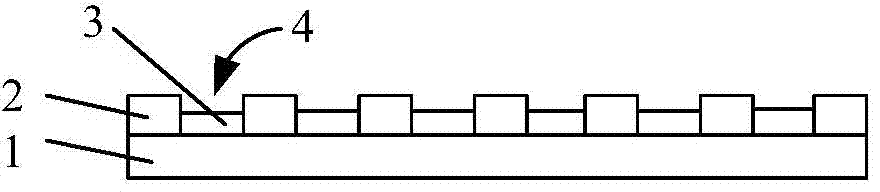
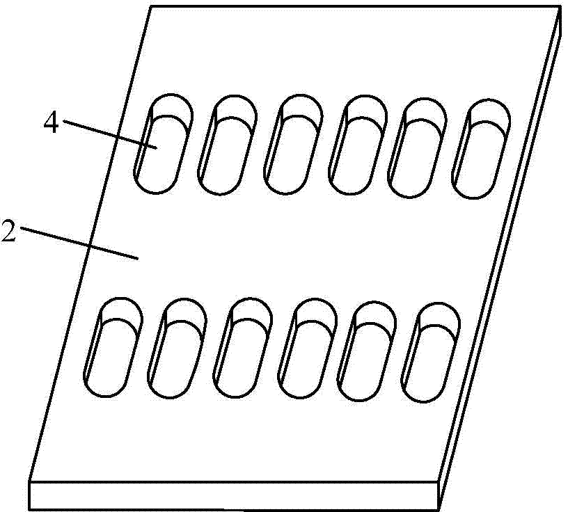
[0077] Figure 5a It is a schematic structural diagram of the pixel defining layer in Embodiment 1 of the present invention, as shown in Figure 5a ...
Embodiment 2
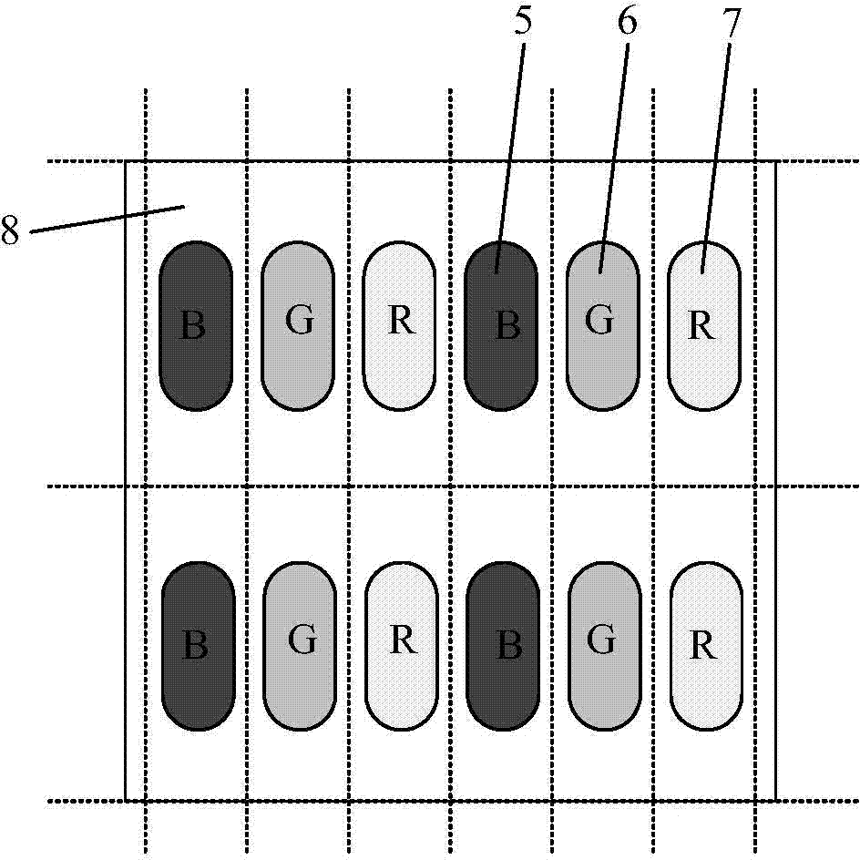
[0094] The electroluminescent device prepared in this embodiment includes electroluminescent layers of three colors, that is, the predetermined colors include: a first color, a second color and a third color.
[0095] Image 6 The flow chart of the manufacturing method of the electroluminescent device provided for the second embodiment of the present invention, such as Image 6 shown, including:
[0096] Step 201: forming a pixel defining layer above the substrate, the pixel defining layer is surrounded by a matrix of pixel openings, at least one horizontally arranged connecting channel is formed on the pixel defining layer, and a row of pixel openings corresponds to two horizontally arranged connecting channels, Two laterally arranged connection channels are respectively located on both sides of the corresponding row of pixel openings, one connection channel is connected to at least two pixel openings in the same row and corresponding to the electroluminescent layer of the f...
Embodiment 3
[0121]The electroluminescent device prepared in this embodiment includes electroluminescent layers of three colors, that is, the predetermined colors include: a first color, a second color and a third color.
[0122] Figure 9 The flowchart of the manufacturing method of the electroluminescent device provided for the third embodiment of the present invention, such as Figure 9 shown, including:
[0123] Step 301: forming a pixel defining layer above the substrate, the pixel defining layer is surrounded by a matrix of pixel openings, at least one vertical connection channel is formed on the pixel defining layer, and a row of pixel openings corresponds to two vertical connection channels, Two vertical connection channels are respectively located on both sides of the pixel opening in the corresponding column, one connection channel is connected to at least two pixel openings in the same column and corresponding to the electroluminescent layer of the first color, and the other co...
PUM
| Property | Measurement | Unit |
|---|---|---|
| Thickness | aaaaa | aaaaa |
Abstract
Description
Claims
Application Information
 - Generate Ideas
- Intellectual Property
- Life Sciences
- Materials
- Tech Scout
- Unparalleled Data Quality
- Higher Quality Content
- 60% Fewer Hallucinations
Browse by: Latest US Patents, China's latest patents, Technical Efficacy Thesaurus, Application Domain, Technology Topic, Popular Technical Reports.
© 2025 PatSnap. All rights reserved.Legal|Privacy policy|Modern Slavery Act Transparency Statement|Sitemap|About US| Contact US: help@patsnap.com