Check patentability & draft patents in minutes with Patsnap Eureka AI!

Gate electrode for nonvolatile three-dimensional semiconductor memory, and preparation method for gate electrode

A non-volatile, gate electrode technology, applied in semiconductor/solid-state device manufacturing, semiconductor devices, electric solid-state devices, etc., can solve problems such as memory cell crosstalk

Active Publication Date: 2015-01-28
HUAZHONG UNIV OF SCI & TECH
View PDF8 Cites 23 Cited by
  • Summary
  • Abstract
  • Description
  • Claims
  • Application Information

AI Technical Summary

Problems solved by technology

[0006] In view of the defects of the prior art, the purpose of the present invention is to provide a gate electrode of a non-volatile three-dimensional semiconductor memory and its preparation method, aiming at solving the problem of crosstalk in the memory cells in the prior art

Method used


Image

  • Gate electrode for nonvolatile three-dimensional semiconductor memory, and preparation method for gate electrode
  • Gate electrode for nonvolatile three-dimensional semiconductor memory, and preparation method for gate electrode
  • Gate electrode for nonvolatile three-dimensional semiconductor memory, and preparation method for gate electrode

Examples


preparation example Construction

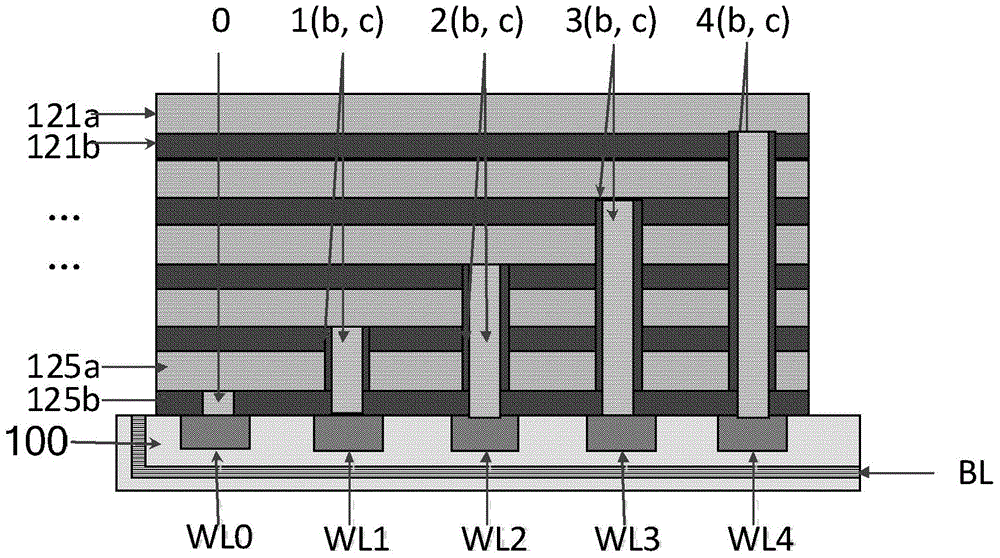
[0078]The preparation method of this novel gate electrode is mainly divided into three types: (1) The first method is a step-by-step downward etching and filling method. This method is mainly to etch downward after each deposition of the insulating layer until the surface of the gate electrode deposited last time is exposed. Moreover, the number of holes etched and filled each time decreases, and the number of holes etched and filled for the first time corresponds to the number of word lines (or the number of gate layers) as N. That is, the first time is N, the second time is N-1, and so on until the last layer of gate electrode is etched and filled with a hole, and the stepped gate electrode structure can be completed. And in each filling process, it is necessary to first fill the sidewall with insulating material and then fill with conductive gate electrode material. This method is applicable to the embodiment in which the gate layer is made of metal material, and the etchi...


PUM


Abstract

The invention discloses a gate electrode for a nonvolatile three-dimensional semiconductor memory, and a preparation method for the gate electrode. The gate electrode comprises n gate electrode units which are sequentially arranged in a step-shaped manner. Each gate electrode unit is in a cylindrical structure, and consists of a connected electrode and an insulating side wall surrounding the connected electrode. The upper surface of the connected electrode is used for connecting a gate layer, and the lower surface of the connected electrode is used for connecting a word line. The invention is suitable for the manufacture of the electrode structure of a connecting gate layer after a front technological step of the word line is completed. The structure is connected with different stacked layers and the corresponding gate layers in a step-shaped manner. In the stacked layers, the gate layer and the gate electrode, which are not corresponding to each other, are isolated from each other through an insulating layer.

Description

technical field [0001] The invention belongs to the technical field of microelectronic devices, and more specifically relates to a gate electrode of a nonvolatile three-dimensional semiconductor memory and a preparation method thereof. Background technique [0002] In order to meet the development of high-efficiency and low-cost microelectronics industry, semiconductor memories need to have higher integration density. High density is critical to reducing the cost of semiconductor products. For traditional two-dimensional and planar semiconductor memories, their integration density mainly depends on the unit area occupied by a single storage device, and the integration degree is very dependent on the quality of the mask process. However, even if expensive process equipment is continuously used to improve the mask process precision, the increase in integration density is still very limited. Especially with the development of Moore's Law, below the 22nm process node, planar s...

Claims


Application Information

Patent Timeline
Patent Type & Authority Applications(China)
IPC IPC(8): H01L27/115H01L21/8247H01L29/423H01L21/28H10B41/27H10B69/00
Inventor 缪向水杨哲童浩
Owner HUAZHONG UNIV OF SCI & TECH
Features
  • R&D
  • Intellectual Property
  • Life Sciences
  • Materials
  • Tech Scout
  • Unparalleled Data Quality
  • Higher Quality Content
  • 60% Fewer Hallucinations
Learn More