Bendable liquid crystal display and manufacturing method thereof
A liquid crystal display, liquid crystal display technology, applied in instruments, optics, nonlinear optics, etc., can solve the problems of not withstand voltage and shock resistance, the display is full of bubbles, the size of the display is thick, etc., to achieve high shock resistance and pressure resistance, not easy to damage. , the effect of improving reliability
- Summary
- Abstract
- Description
- Claims
- Application Information
AI Technical Summary
Problems solved by technology
Method used
Image
Examples
Embodiment 1
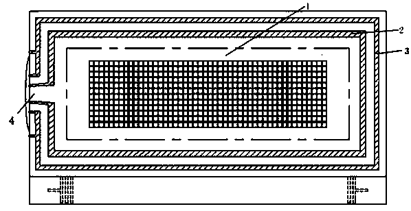
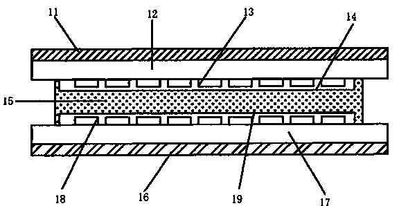
[0035] In this embodiment, it includes a liquid crystal display assembly 1 and a frame sealing glue assembly, the sealing glue assembly is arranged at the edges around the liquid crystal display assembly and separates the liquid crystal display assembly from the outside; the frame sealing plate The component includes two layers of frame sealant arranged at intervals, the first layer of frame sealant 2 and the second layer of frame sealant 3, the first layer of frame sealant 2 and the second layer of frame sealant 3 are resin glue; The frame sealant 2 and the second layer of frame sealant 3 are provided with an opening 4 for pouring liquid crystals, and the opening 4 is sealed by a sealant, and the sealant includes UV curable resin glue.
[0036] In this example, the frame sealant is epoxy resin glue. This example only illustrates the material of the frame sealant, and does not limit the protection of the material of the frame sealant in the present invention. The frame sealant ...
Embodiment 2
[0049] This embodiment provides a method for manufacturing a flexible liquid crystal display, the process of which is:
[0050] Respectively engraving required electrode patterns on the first substrate and the second substrate to form the first electrode and the second electrode;
[0051] Coating an alignment film on the electrodes of the first substrate and the second substrate respectively, heating and curing them, and rubbing the alignment films of the first electrode and the second electrode with flannelette to obtain the desired liquid crystal alignment direction;
[0052] Set conduction points on the first electrode by screen-printing conductive gold balls, and spray spacer balls on the first and / or second electrodes;
[0053] Apply multiple layers of epoxy resin glue between the first substrate and the second substrate, each layer of epoxy resin glue leaves a liquid crystal pouring port at the same position, attach the first substrate and the second substrate together, ...
PUM
| Property | Measurement | Unit |
|---|---|---|
| Thickness | aaaaa | aaaaa |
| Thickness | aaaaa | aaaaa |
Abstract
Description
Claims
Application Information

