
OLED (Organic Light Emitting Diode) pixel arrangement structure

A pixel arrangement and pixel technology, which is applied in the field of OLED display, can solve the problems of difficult metal mask evaporation, obvious moiré effect, and deterioration of oblique sawtooth, and achieve the effect of saving process cost, reducing process difficulty, and increasing aperture ratio

Inactive Publication Date: 2015-02-04
EVERDISPLAY OPTRONICS (SHANGHAI) CO LTD
View PDF2 Cites 59 Cited by
  • Summary
  • Abstract
  • Description
  • Claims
  • Application Information

AI Technical Summary

Problems solved by technology

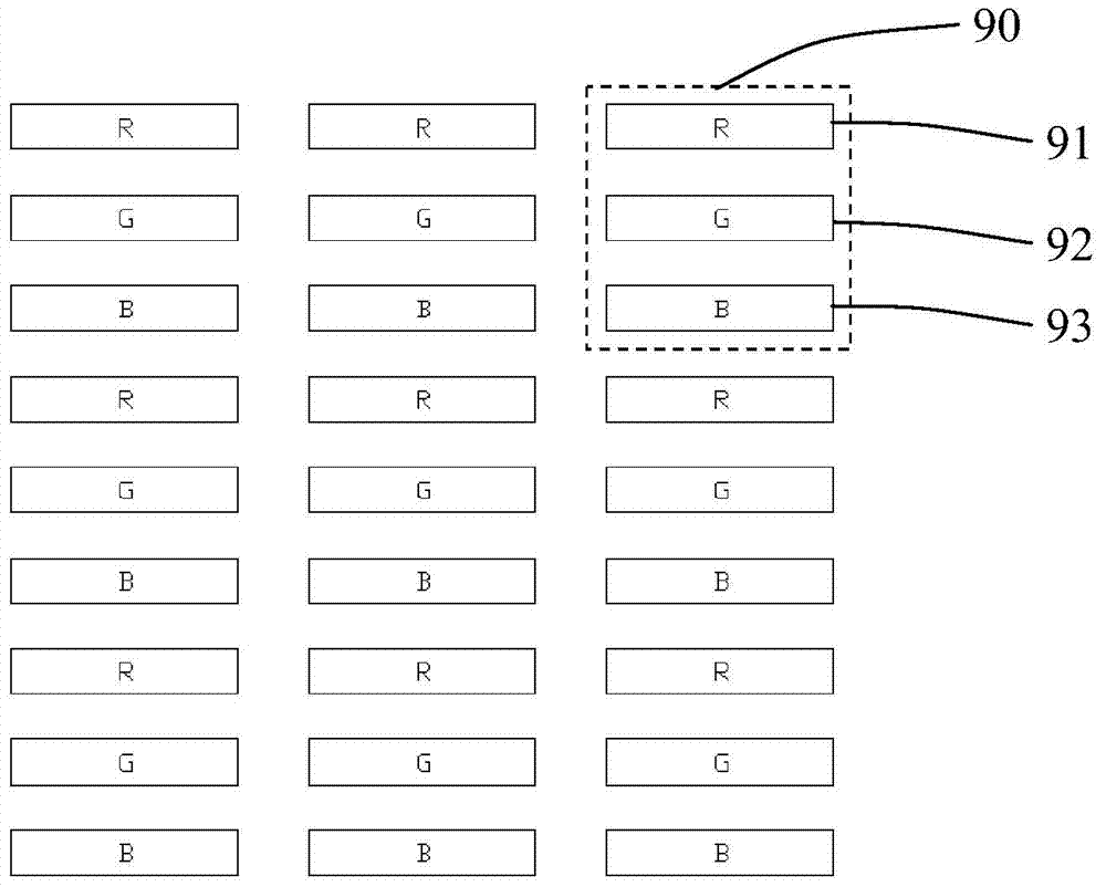
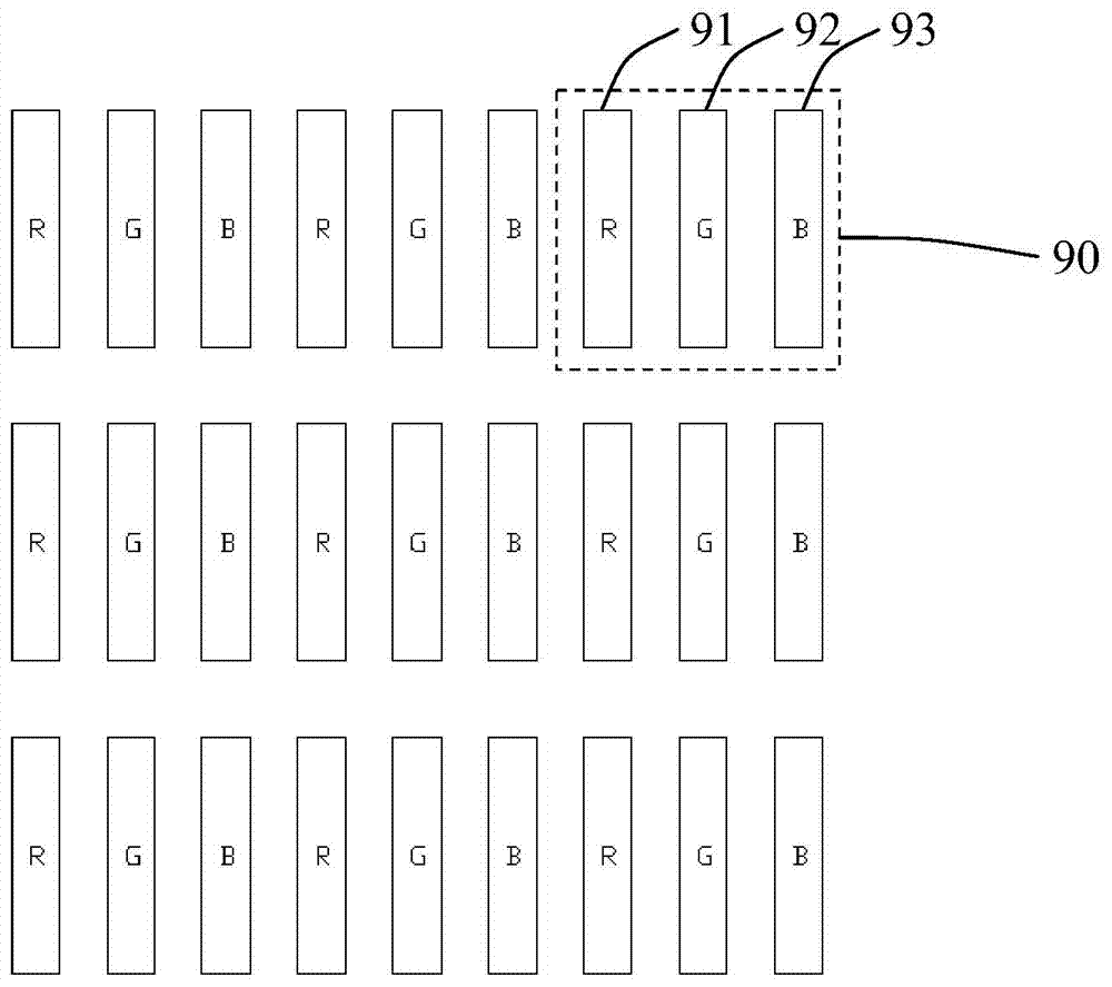
However, it is difficult for existing OLEDs to meet the high-resolution and high-brightness requirements of electronic devices for display screens, because when the resolution of OLEDs reaches more than 300PPI (pixels per inch), the pixel arrangement structure of traditional RGB stripes is difficult to achieve. Evaporate organic light-emitting materials with a metal mask, and due to the low aperture ratio, the current density injected into the OLED is high, and it is necessary to choose a compromise between brightness and life
In order to improve this problem in the industry, although some manufacturers have proposed a more efficient pixel arrangement called "PenTileRGB", but this arrangement has problems such as increased image crosstalk, obvious moiré effect, and deterioration of oblique line aliasing.

Method used


Image

  • OLED (Organic Light Emitting Diode) pixel arrangement structure
  • OLED (Organic Light Emitting Diode) pixel arrangement structure
  • OLED (Organic Light Emitting Diode) pixel arrangement structure

Examples


Embodiment 1

[0061] Figure 4 It is a schematic diagram of the first embodiment of the OLED pixel arrangement structure of the present invention, such as Figure 4 As shown, in Embodiment 1, the first direction is the row direction (the X direction shown in the figure), and the second direction is the column direction (the Y direction is shown in the figure). In this embodiment, the OLED pixel arrangement structure includes:

[0062] A plurality of first sub-pixel rows 50, the first sub-pixel row 50 includes a first R sub-pixel group 10a, a first G sub-pixel group 20a, and a first B sub-pixel group 30a arranged in sequence along the row direction;

[0063] A plurality of second sub-pixel rows 60, the second sub-pixel row 60 includes a second R sub-pixel group 10b, a second G sub-pixel group 20b, and a second B sub-pixel group 30b arranged in sequence along the row direction;

[0064] The first sub-pixel row 50 and the second sub-pixel row 60 are arranged at intervals, and the first R sub...

Embodiment 2

[0074] Figure 7 It is a schematic diagram of the second embodiment of the OLED pixel arrangement structure of the present invention. Such as Figure 7 As shown, in Embodiment 2, the first direction is the column direction (the Y direction shown in the figure), and the second direction is the row direction (the X direction is shown in the figure). In this embodiment, the OLED pixel arrangement structure includes:

[0075] A plurality of first sub-pixel columns 70, the first sub-pixel column 70 includes a first R sub-pixel group 10c, a first G sub-pixel group 20c, and a first B sub-pixel group 30c arranged in sequence along the row direction;

[0076] A plurality of second sub-pixel columns 80, the second sub-pixel columns 80 include a second R sub-pixel group 10d, a second G sub-pixel group 20d, and a second B sub-pixel group 30d arranged in sequence along the row direction;

[0077] The first sub-pixel row 70 and the second sub-pixel row 80 are arranged at intervals, the f...


PUM


Abstract

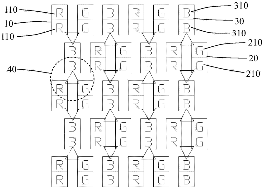
The invention provides an OLED (Organic Light Emitting Diode) pixel arrangement structure. The OLED pixel arrangement structure comprises an R sub-pixel group, a G sub-pixel group and a B sub-pixel group; the R sub-pixel group is formed by plural R sub-pixels; the G sub-pixel group is formed by plural G sub-pixels; the B sub-pixel group is formed by plural B sub-pixels; the R sub-pixel group, the G sub-pixel group and the B sub-pixel group are arranged separately to enable every adjacent R sub-pixel, G sub-pixel and B sub-pixel which are arranged in the R sub-pixel group, the G sub-pixel group and the B sub-pixel group respectively to form a pixel. According to the OLED pixel arrangement structure, the same color of sub-pixels are gathered into a sub-pixel unit and accordingly the opening rate of a metal mask template can be improved under the same resolution of an OLED display screen in comparison with the single sub-pixel in the prior art, the problem that the manufacture of the metal mask template is difficult is solved, or every sub-pixel in one sub-pixel unit can be small under the same opening rate of the metal mask template so as to well improve the resolution of the OLED display screen.

Description

technical field [0001] The invention relates to OLED display technology, in particular to an OLED pixel arrangement structure. Background technique [0002] In flat panel display technology, Organic Light-Emitting Diode (OLED) displays are famous for their thinness, active light emission, fast response speed, wide viewing angle, rich colors and high brightness, low power consumption, and high and low temperature resistance. It is recognized by the industry as the third generation of display technology after liquid crystal display (LCD). According to the driving method, OLED is divided into passive OLED (Passive Matrix OLED, PMOLED) and active OLED (Active Matrix OLED, AMOLED). PMOLED is also called passive matrix OLED, and AMOLED is also called active matrix OLED. PMOLED can only To produce small-sized, low-resolution display panels, AMOLED can realize large-sized, high-resolution panels because it integrates a thin-film transistor (TFT) and a capacitor in each pixel and ma...

Claims


Application Information

Patent Timeline
Patent Type & Authority Applications(China)
IPC IPC(8): H01L27/32
CPCH10K59/353
Inventor 冯佑雄
Owner EVERDISPLAY OPTRONICS (SHANGHAI) CO LTD
Learn More