
A chip-on-board substrate and its manufacturing process

A manufacturing process and substrate technology, applied in the field of LED lighting equipment, can solve problems such as poor anti-high voltage characteristics, affecting the lighting effect of LED lamps, and limiting the maximum power-on voltage of on-board chips, so as to avoid discharge, improve lighting effects, and eliminate maximum power-on The effect of voltage limitation

Active Publication Date: 2018-12-04
惠州市华阳光电技术有限公司
View PDF2 Cites 0 Cited by
  • Summary
  • Abstract
  • Description
  • Claims
  • Application Information

AI Technical Summary

Problems solved by technology

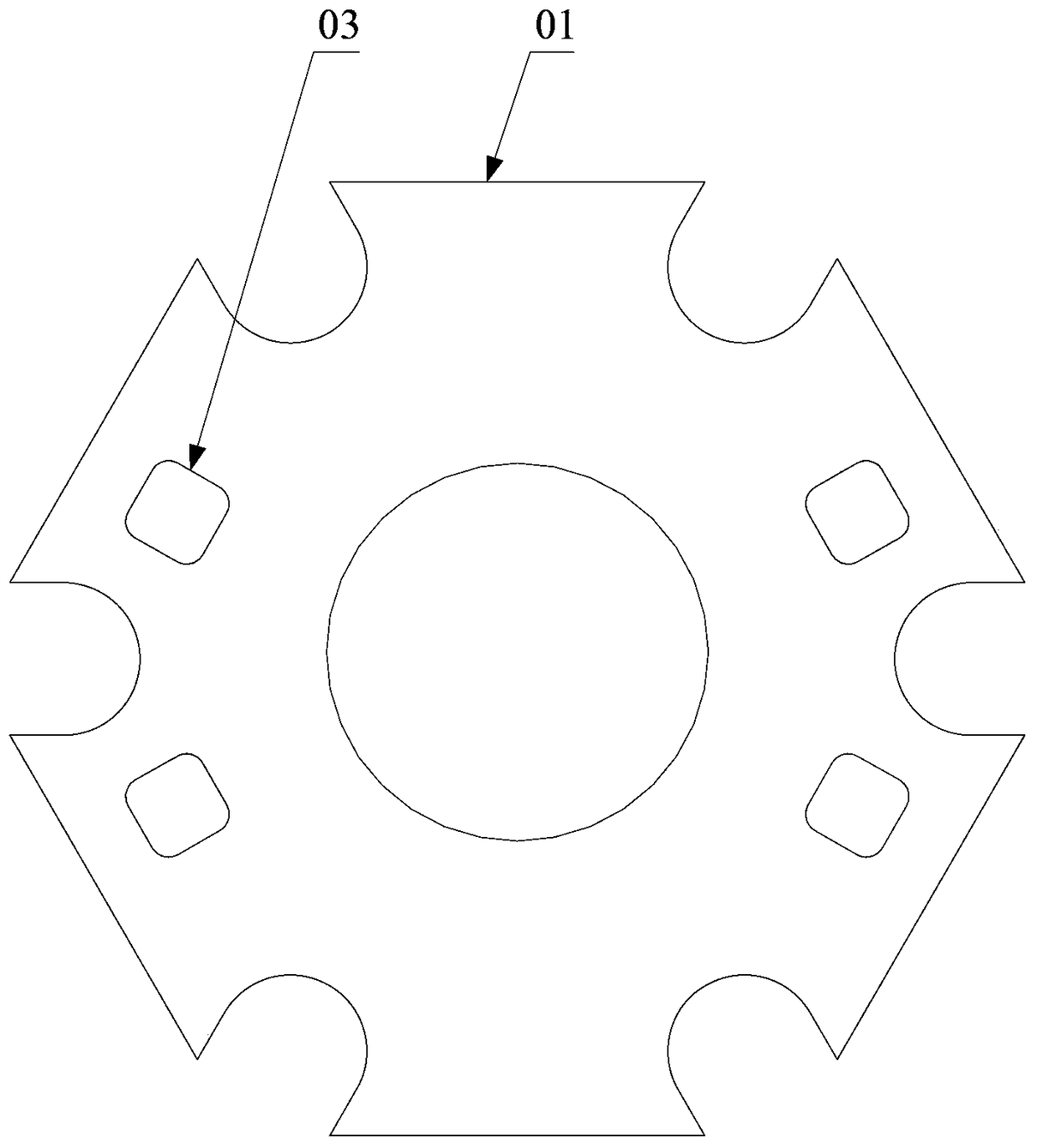
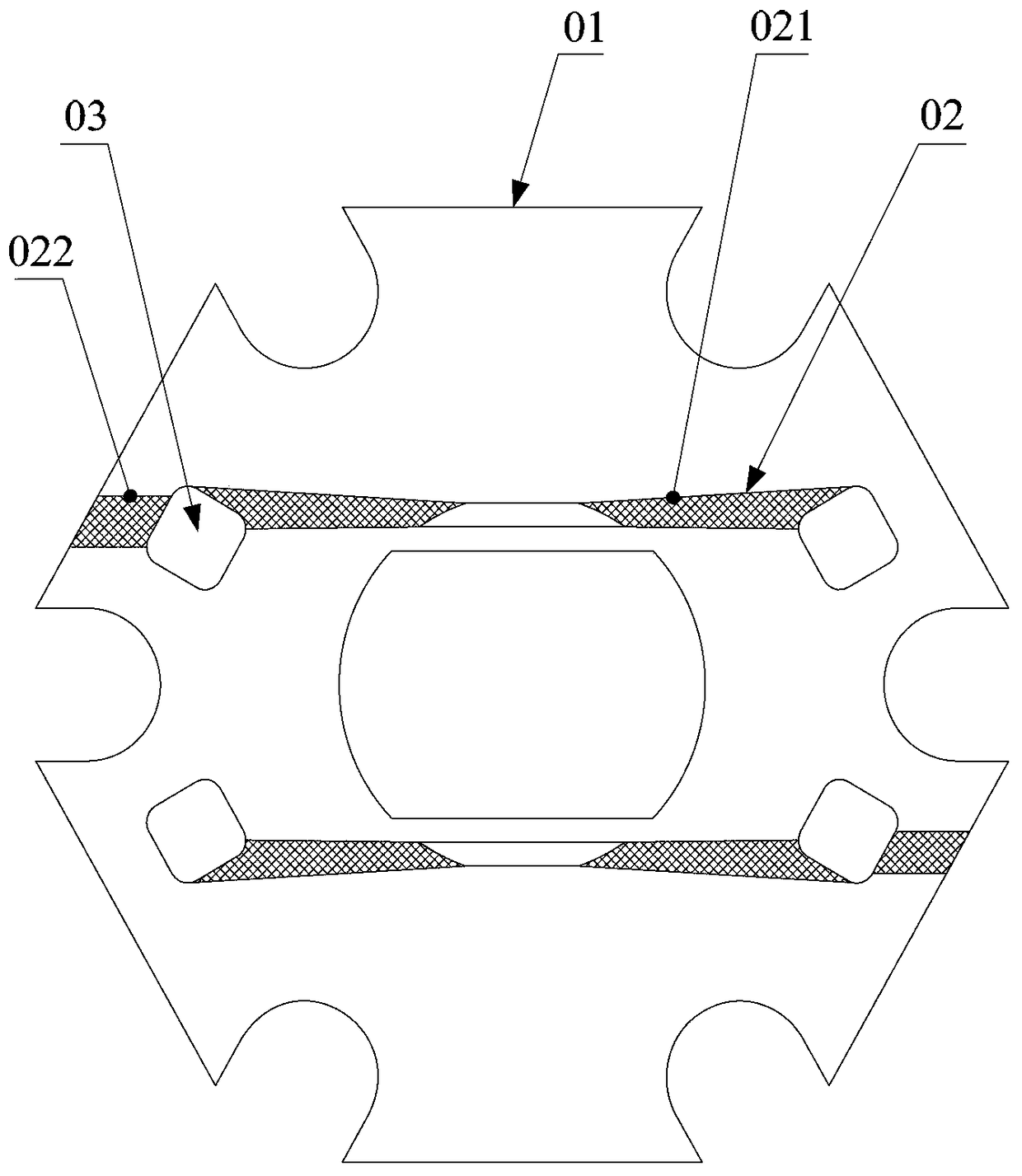
[0004] However, in the prior art, in addition to the connecting portion 021 arranged between different chips 03, the electroplating lead 02 also has an extension portion 022, which extends to the vicinity of the bottom edge of the substrate 01, and is used for The chip on board of the LED lamp is set on the copper seat. When the chip on the board is powered on, the extension part 022 of the plating lead 02 near the bottom edge of the substrate 01 is very close to the bottom copper seat, so it is easy to contact with the bottom copper seat. Discharge occurs in the seat, which limits the maximum power-on voltage of the chip on the board, and the anti-high voltage characteristic is poor, which in turn affects the lighting effect of the LED lamp

Method used


Image

  • A chip-on-board substrate and its manufacturing process
  • A chip-on-board substrate and its manufacturing process
  • A chip-on-board substrate and its manufacturing process

Examples


Embodiment Construction

[0028] The invention provides a chip-on-board substrate manufacturing process, which can avoid discharge between the electroplating lead wire and the copper seat, thereby improving the lighting effect of the LED lamp.

[0029] The following will clearly and completely describe the technical solutions in the embodiments of the present invention with reference to the accompanying drawings in the embodiments of the present invention. Obviously, the described embodiments are only some, not all, embodiments of the present invention. Based on the embodiments of the present invention, all other embodiments obtained by persons of ordinary skill in the art without making creative efforts belong to the protection scope of the present invention.

[0030] Such as Figure 4 As shown, the chip-on-board substrate manufacturing process provided by the embodiment of the present invention includes the following steps:

[0031] S101, bonding an insulating layer on the base material;

[0032] S...


PUM


Abstract

The invention provides a manufacturing process of a substrate of a chip on board. The manufacturing process comprises the following steps: arranging an insulating layer on the substrate; etching the insulating layer to form a circuit; arranging an electroplated lead with a connection part and an extension part; electroplating the substrate; removing the extension part by using the etching process. According to the manufacturing process of the substrate of the chip on board provided by the invention, since the extension part of the electroplated lead close to the bottom edge of the substrate is etched to be removed, the phenomenon of discharge between the electroplated lead and a copper seat is avoided, the limitation to the highest power-on voltage of the chip on board is eliminated, the high voltage resistance characteristic is improved, and the lighting effect of an LED (Light Emitting Diode) lamp is further improved. The invention also provides the substrate of the chip on board manufactured by using the manufacturing process.

Description

technical field [0001] The present invention relates to the technical field of LED lighting equipment, and more specifically, relates to a chip-on-board substrate manufacturing process, and the present invention also relates to a chip-on-board substrate manufactured by the manufacturing process. Background technique [0002] With the continuous development of semiconductor lighting technology, more and more LED (English Light-Emitting Diode abbreviation, light-emitting diode) lights have entered various lighting fields. [0003] The main light-emitting part of the LED lamp is a chip-on-board provided with LEDs, and the substrate 01 of the chip-on-board (such as figure 1 and figure 2 ) with an aluminum base as the base material. In the production process, it is first necessary to bond an insulating layer on the aluminum base or copper base, and then etch the copper on the insulating layer to form a circuit, and then through electroplating The silver plating operation is pe...

Claims


Application Information

Patent Timeline
Patent Type & Authority Patents(China)
IPC IPC(8): H01L33/48H01L33/62
CPCH01L33/62H01L33/641H01L2933/0066H01L2933/0075
Inventor 刘云王峰
Owner 惠州市华阳光电技术有限公司
Learn More