Main node circuit for plastic optical fiber communication
A technology of plastic optical fiber and main node, applied in the field of electric energy information collection system, can solve the problems of large space, high cost, weak anti-electromagnetic interference ability, etc., and achieve the effect of promoting application
- Summary
- Abstract
- Description
- Claims
- Application Information
AI Technical Summary
Problems solved by technology
Method used
Image

Examples
Embodiment Construction
[0024] The present invention will be further elaborated below in conjunction with the accompanying drawings.
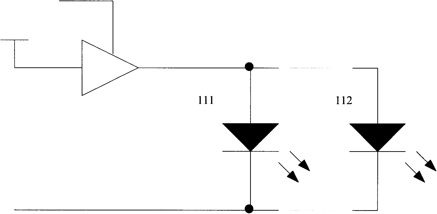
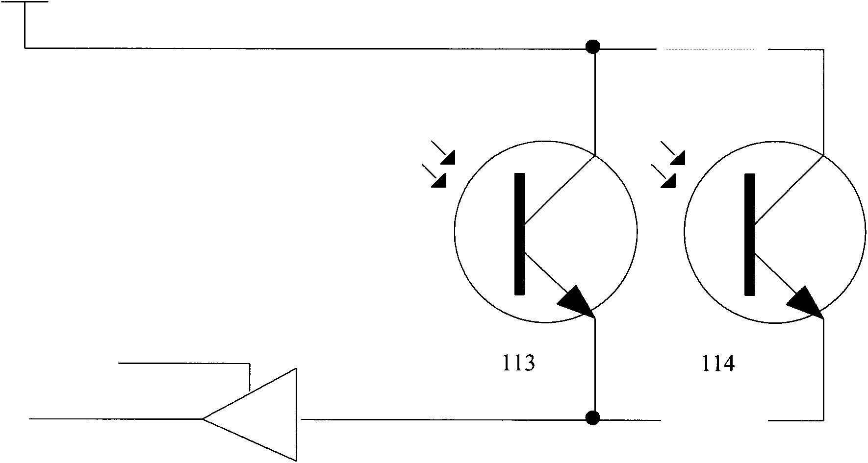
[0025] see figure 1 and figure 2 , when the present invention constructs a plastic optical fiber communication system, both the master node and the slave node are equipped with a dual-channel photoelectric transceiver interface, that is to say, each node includes two light-emitting diodes 111, 112 for sending optical signals , and includes two photosensitive devices 113, 114 for receiving light signals.
[0026] Implementation one
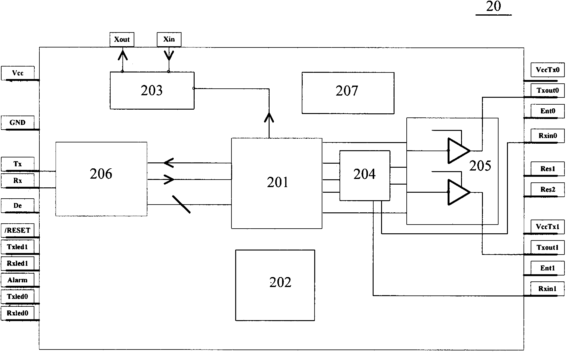
[0027] The present invention proposes a master node circuit 20 for plastic optical fiber communication, see image 3 , which includes integrated: a control unit 201, which includes an 80c51 microprocessor core; a storage unit 202, which includes a 16K byte flash memory, a 1 / 2K byte Flash data memory, and a 1 / 2K byte SRAM And 256 bytes of RAM space; a time base circuit unit 203, used to provide the control unit clock reference and NRZ ...
PUM
 Abstract
Description
Claims
Application Information
 - R&D
- Intellectual Property
- Life Sciences
- Materials
- Tech Scout
- Unparalleled Data Quality
- Higher Quality Content
- 60% Fewer Hallucinations
Browse by: Latest US Patents, China's latest patents, Technical Efficacy Thesaurus, Application Domain, Technology Topic, Popular Technical Reports.
© 2025 PatSnap. All rights reserved.Legal|Privacy policy|Modern Slavery Act Transparency Statement|Sitemap|About US| Contact US: help@patsnap.com