Partially-depleted silicon-on-insulator triode structure

A technology of silicon on insulator and triode, which is applied in the direction of transistors, semiconductor devices, electrical components, etc., can solve the problems of poor performance of parasitic triodes in silicon MOSFET structures, and achieve good tube performance, easy layout and wiring, and large collector area Effect

Inactive Publication Date: 2015-02-18
SHANGHAI HUAHONG GRACE SEMICON MFG CORP
View PDF5 Cites 0 Cited by
  • Summary
  • Abstract
  • Description
  • Claims
  • Application Information

AI Technical Summary

Problems solved by technology

[0003] Figure 1 to Figure 3 The performance of the parasitic transistor of the conventional partially depleted silicon-on-insulator MOSFET structure shown is not good

Method used


Image

  • Partially-depleted silicon-on-insulator triode structure
  • Partially-depleted silicon-on-insulator triode structure
  • Partially-depleted silicon-on-insulator triode structure

Examples


Embodiment Construction

[0020] In order to make the content of the present invention clearer and easier to understand, the content of the present invention will be described in detail below in conjunction with specific embodiments and accompanying drawings.

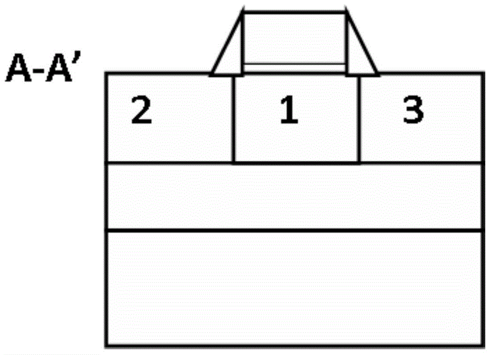
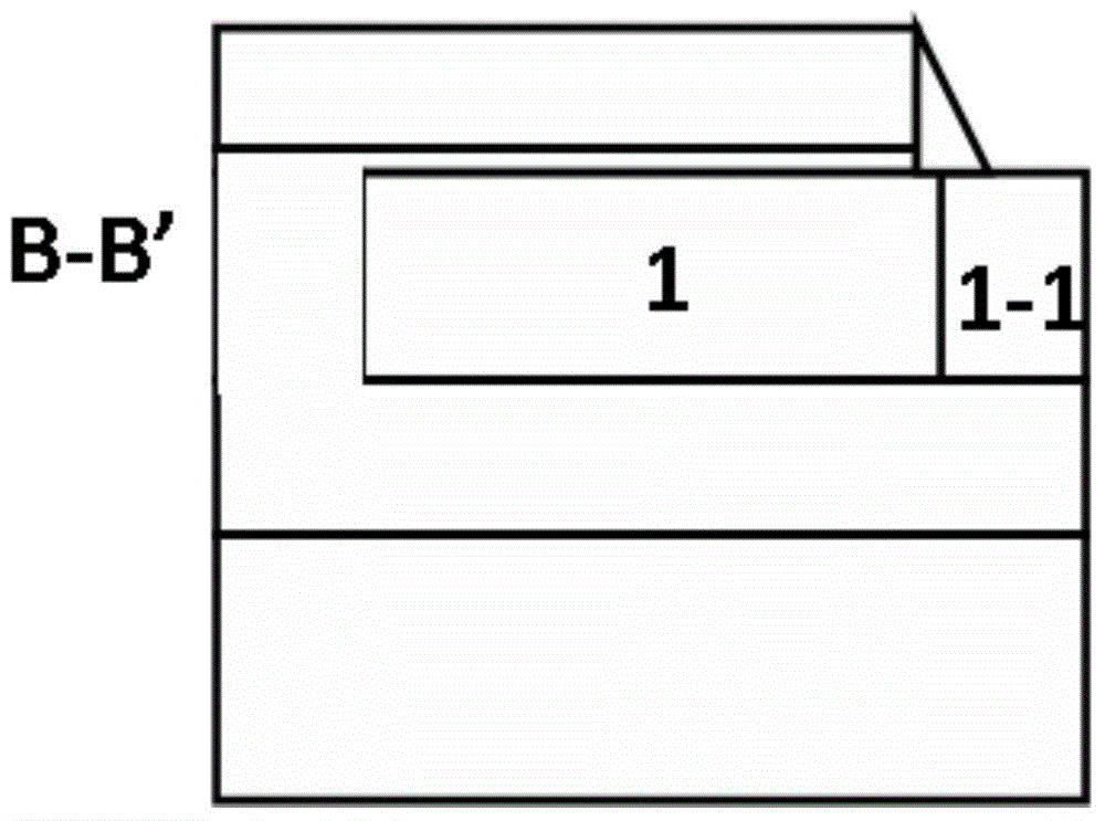
[0021] Figure 4 A schematic cross-sectional view of a partially depleted silicon-on-insulator transistor structure according to a preferred embodiment of the present invention is shown schematically.

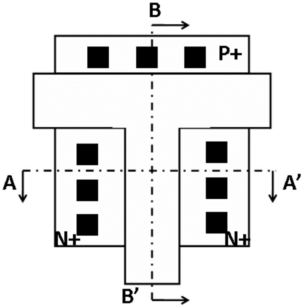
[0022] Such as Figure 4 As shown, the partially depleted silicon-on-insulator transistor structure according to the preferred embodiment of the present invention includes: a buried oxide layer 200 (ie SOI silicon wafer) arranged on a substrate 100 (such as a silicon substrate), and a buried oxide layer 200 arranged on the buried oxide layer 200 The upper collector region 600 (preferably, the doping type of the collector region 600 is N-type doping, such as phosphorus doping, arsenic doping), the base region 500 arranged above the collector regi...


PUM


Abstract

The invention provides a partially-depleted silicon-on-insulator triode structure. The partially-depleted silicon-on-insulator triode structure comprises a buried oxygen layer, a collector electrode region, a base region, an ultra-shallow trench isolation region, a base electrode region and a collector electrode contact region, wherein the buried oxygen layer is arranged on a substrate, the collector electrode region is arranged on the buried oxygen layer, the base region is located on the collector electrode region, the ultra-shallow trench isolation region and the base electrode region are arranged on the two sides of the base region respectively, and the collector electrode contact region is arranged on the side, opposite to the base region, of the ultra-shallow trench isolation region; the doping concentration of the collector electrode contact region is larger than that of the collector electrode region, the collector electrode region is connected with the collector electrode contact region, and the collector electrode contact region, the ultra-shallow trench isolation region, the base region and the base electrode region are located on the surface of a silicon wafer. Moreover, the partially-depleted silicon-on-insulator triode structure further comprises a polycrystalline silicon emitting electrode arranged on the surface of the silicon wafer.

Description

technical field [0001] The invention relates to the field of semiconductor manufacturing, more specifically, the invention relates to a partially depleted silicon-on-insulator (PD-SOI, partially-depleted silicon-on-insulator) transistor structure. Background technique [0002] Due to the thinner top layer of partially depleted silicon-on-insulator, the formed triode has poor characteristics, such as insufficient amplification capability. figure 1 Schematically showing a partially depleted silicon-on-insulator transistor according to the prior art, figure 2 Schematically showing a first cross-sectional structure diagram along the line A-A' of a partially depleted silicon-on-insulator transistor according to the prior art, image 3 Schematically shows a second cross-sectional structural view along line B-B' of a partially depleted SOI transistor according to the prior art. Such as Figure 1 to Figure 3 As shown in FIG. 1 , the structure of base 1 , collector 2 and emitter ...

Claims


Application Information

Patent Timeline
Patent Type & Authority Applications(China)
IPC IPC(8): H01L29/73H01L29/08
CPCH01L29/73H01L29/0821
Inventor 刘张李
Owner SHANGHAI HUAHONG GRACE SEMICON MFG CORP
Why Eureka
Try Eureka