
Semiconductor-metal contact resistivity detection method and array substrate

A technology of metal contact and detection method, applied in the direction of semiconductor devices, semiconductor/solid-state device parts, measuring resistance/reactance/impedance, etc., can solve problems such as poor accuracy and achieve accurate results

Inactive Publication Date: 2015-03-11
HEFEI BOE OPTOELECTRONICS TECH +1
View PDF4 Cites 9 Cited by
  • Summary
  • Abstract
  • Description
  • Claims
  • Application Information

AI Technical Summary

Problems solved by technology

[0004] The present invention aims at the problem of poor accuracy of the existing method for detecting the contact resistance of the active area of ​​the array substrate, and provides a simple and accurate method for detecting the contact resistance of the semiconductor layer

Method used


Image

  • Semiconductor-metal contact resistivity detection method and array substrate
  • Semiconductor-metal contact resistivity detection method and array substrate
  • Semiconductor-metal contact resistivity detection method and array substrate

Examples


Embodiment 1

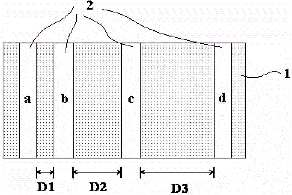
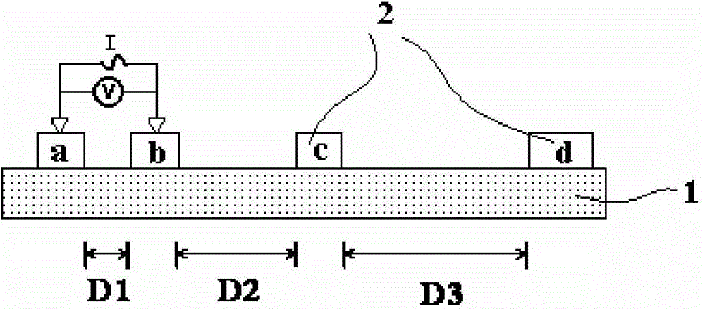
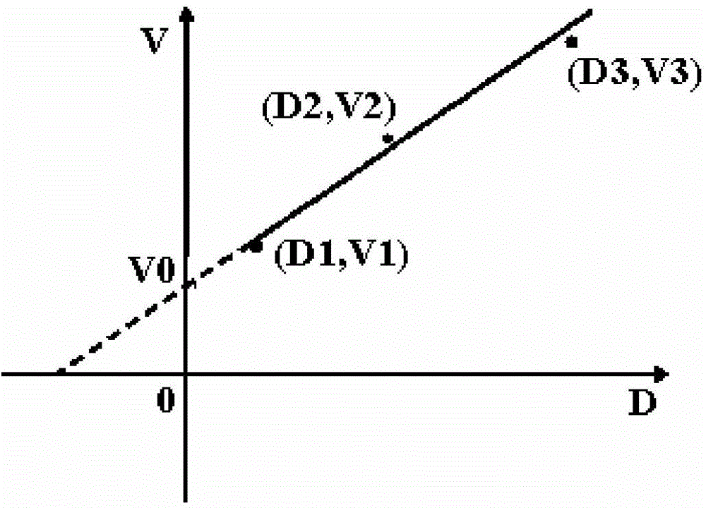
[0032] Such as Figure 1 to Figure 3 As shown, this embodiment provides a semiconductor-metal contact resistivity detection method.

[0033] Wherein, on the semiconductor layer 1 used for the above detection, at least three metal strips 2 with the same shape and size, parallel to each other, spaced apart, and opposite to each other are provided.

[0034] That is, if figure 1 , figure 2 As shown, on the semiconductor layer 1 to be detected, there are a plurality of metal strips 2, the shapes and sizes of these metals are exactly the same, and they are parallel to each other, and each metal strip 2 is arranged in sequence along the same direction, and the adjacent metal strips 2 separated by a certain distance.

[0035] The above detection methods specifically include:

[0036] S100. Optionally, if there is no metal strip 2 on the semiconductor layer 1 to be detected, the metal strip 2 is first formed on the semiconductor layer 1 through a patterning process.

[0037] S101...


PUM


Abstract

The invention provides a semiconductor-metal contact resistivity detection method and an array substrate, belongs to the technical field of array substrate detection and can solve the problem that an existing array substrate active area contact resistivity detection method is low in accuracy. In the semiconductor-metal contact resistivity detection method, at least three metal strips which are identical in shape and size, parallel to one another and arranged oppositely at intervals are arranged on a to-be-detected semiconductor layer. The semiconductor-metal contact resistivity detection method includes determining multiple detection groups, wherein each detection group includes two metal strips, and distances between two opposite surfaces of two metal strips of different detection groups are different; sequentially supplying current between the metal strips of each detection group, and detecting voltage of the metal strips respectively; calculating semiconductor-metal contact resistivity according to current and voltage between the metal strip of each detection group. The semiconductor-metal contact resistivity detection method can be used for detecting contact resistance between an active area and a source drain electrode of a thin-film transistor of the array substrate.

Description

technical field [0001] The invention belongs to the technical field of array substrate detection, and in particular relates to a semiconductor-metal contact resistivity detection method and an array substrate. Background technique [0002] In array substrates of organic light emitting diode (OLED) display devices, liquid crystal display devices, etc., a large number of thin film transistors are provided. The active region of the thin film transistor is composed of semiconductor, and the contact resistance between the semiconductor layer (active region) and the metal source and drain has an important influence on the performance of the thin film transistor. In order to ensure product quality, the contact resistance between the active area of ​​the array substrate and the source and drain electrodes should be detected. [0003] The existing semiconductor-metal contact resistance (rate) detection method uses a commercially available four-probe contact resistance meter to direc...

Claims


Application Information

Patent Timeline
IPC IPC(8): G01R27/08H01L23/544
Inventor 李纪陈传宝
Owner HEFEI BOE OPTOELECTRONICS TECH
Learn More