An OLED device structure and 3D printing technology based multiple-spray-head printing method thereof

A device structure, multi-nozzle technology, applied in the direction of electric solid device, semiconductor device, semiconductor/solid state device manufacturing, etc., can solve the problems of reducing production cost, troublesome and time-consuming filling of layer-by-layer printing materials, etc., to reduce working time. Effect

Inactive Publication Date: 2015-03-11
FUZHOU UNIV
View PDF4 Cites 15 Cited by
  • Summary
  • Abstract
  • Description
  • Claims
  • Application Information

AI Technical Summary

Problems solved by technology

[0003] In view of the above problems, the present invention provides an OLED device structure and its multi-nozzle printing method based on 3D printing technology. The realization of the OLED device and packaging can be achieved by using multi-nozzles to simultaneously print each layer of material and heat curing technology, which combines the The advantages of 3D printing solve the problems of layer-by-layer printing material loading and complicated procedures, and can realize one-time molding of OLED devices and packaging, greatly reducing the preparation cost and solving the time-consuming problem

Method used


Image

  • An OLED device structure and 3D printing technology based multiple-spray-head printing method thereof
  • An OLED device structure and 3D printing technology based multiple-spray-head printing method thereof
  • An OLED device structure and 3D printing technology based multiple-spray-head printing method thereof

Examples


Embodiment Construction

[0025] In order to make the above-mentioned features and advantages of the present invention more comprehensible, the following specific embodiments are described in detail in conjunction with the accompanying drawings.

[0026] The present invention will be further described in detail through specific examples below.

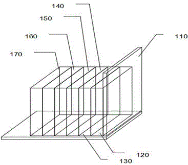
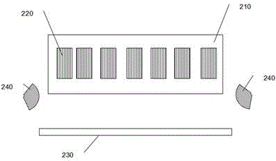
[0027] refer to Figure 1 to Figure 5 , The invention relates to an OLED device structure, comprising a glass substrate arranged on the bottom layer, on which an anode layer, a hole transport layer, an organic light-emitting layer, an electron injection buffer layer, a cathode layer and an encapsulation film layer are sequentially arranged.

[0028] The above-mentioned anode layer is made of ITO powder; the hole transport layer is made of NPB powder, TPD powder or a mixture of two kinds; the organic light-emitting layer is made of Alq 3 powder; the electron injection buffer layer is made of LiF powder; the cathode layer is made of Al powder, Ag powder or a mix...


PUM


Abstract

The invention aims to provide an OLED device structure including a glass substrate arranged in a bottom layer. The OLED device structure is characterized in that an anode layer, a hole transport layer, an organic light emitting layer, an electron injection buffer layer, a cathode layer and an encapsulation thin film layer are arranged in turn on the glass substrate. In the invention, a print head is provided with multiple spray heads for simultaneous printing, three-dimensional models of an OLED device and a package film are pre-designed by a computer, scanning paths of the structure of each layer are positioned precisely on a heating substrate, and then the OLED device is printed, and a heating process is performed by a heating solidification device during printing. The method is simplified as compared with the traditional device printing method, and can be used to carry out the moulding and packaging of the device by one time. The method eliminates troubles of repeatedly filling materials, and reduces greatly working hours. The moulded device rotates 90 degrees as compared with a device traditionally printed layer upon layer, and the film package of the OLED device is realized.

Description

technical field [0001] The invention relates to an OLED device structure and a multi-nozzle printing method based on 3D printing technology, and belongs to the technical field of OLED rapid manufacturing. Background technique [0002] In recent years, organic electroluminescence (OLED) has gradually become a technology that has attracted wide attention at home and abroad. With features such as low profile and bendable panels, OLEDs are likely to become the next generation of mainstream flat-panel displays. The traditional OLED preparation process mainly adopts vacuum evaporation and spin coating process. With the development of technology, some technologies of layer-by-layer printing OLED devices have also appeared, but this technology has micro-spray heads that require multiple state materials and cannot be used once. Molding disadvantages. Contents of the invention [0003] In view of the above problems, the present invention provides an OLED device structure and its m...

Claims


Application Information

Patent Timeline
Patent Type & Authority Applications(China)
IPC IPC(8): H01L51/52H01L51/54H01L51/56
CPCH10K71/135H10K50/00H10K71/00
Inventor 李福山郭太良聂晨曾群英吴家祺
Owner FUZHOU UNIV
Why Eureka
Try Eureka