Method for packaging multi-laminated multi-chip on flexible circuit board and packaging chipset

A flexible circuit substrate, multi-chip packaging technology, applied in the direction of circuits, electrical components, electrical solid devices, etc., can solve the problems of mutual interference of signals, the inability of the size chip packaging to meet the requirements, and the incompatibility between the packaging position and the installation point.

Inactive Publication Date: 2010-09-29
SHENZHEN DANBOND TECH
View PDF6 Cites 13 Cited by
  • Summary
  • Abstract
  • Description
  • Claims
  • Application Information

AI Technical Summary

Problems solved by technology

[0004] In U.S. Patent No. 6,576,992, the chip stacked integrated circuit package uses FBGA (Fine-Pitch Ball Grid Array: Fine-Pitch Ball Grid Array Package, or CSP) technology, because in this patent, the circuit substrate is directly folded when the chip is packaged, so that it is easy to use Substrate wires and packages are damaged, and the time difference between wire signals connecting different chips makes the signals interfere with each other and affects the quality
In US6225688, due to the large difference in the thermal expansion coefficient (CTE) of the flexible substrate, the amount of deformation incre

Method used


Image

  • Method for packaging multi-laminated multi-chip on flexible circuit board and packaging chipset
  • Method for packaging multi-laminated multi-chip on flexible circuit board and packaging chipset
  • Method for packaging multi-laminated multi-chip on flexible circuit board and packaging chipset

Examples


Embodiment Construction

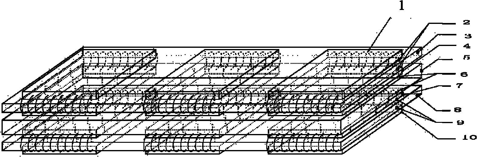
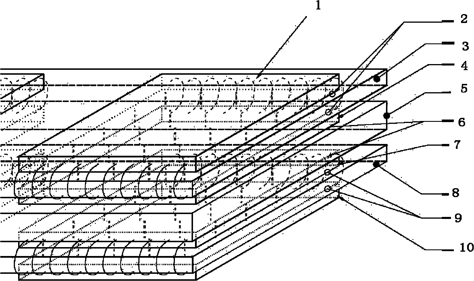
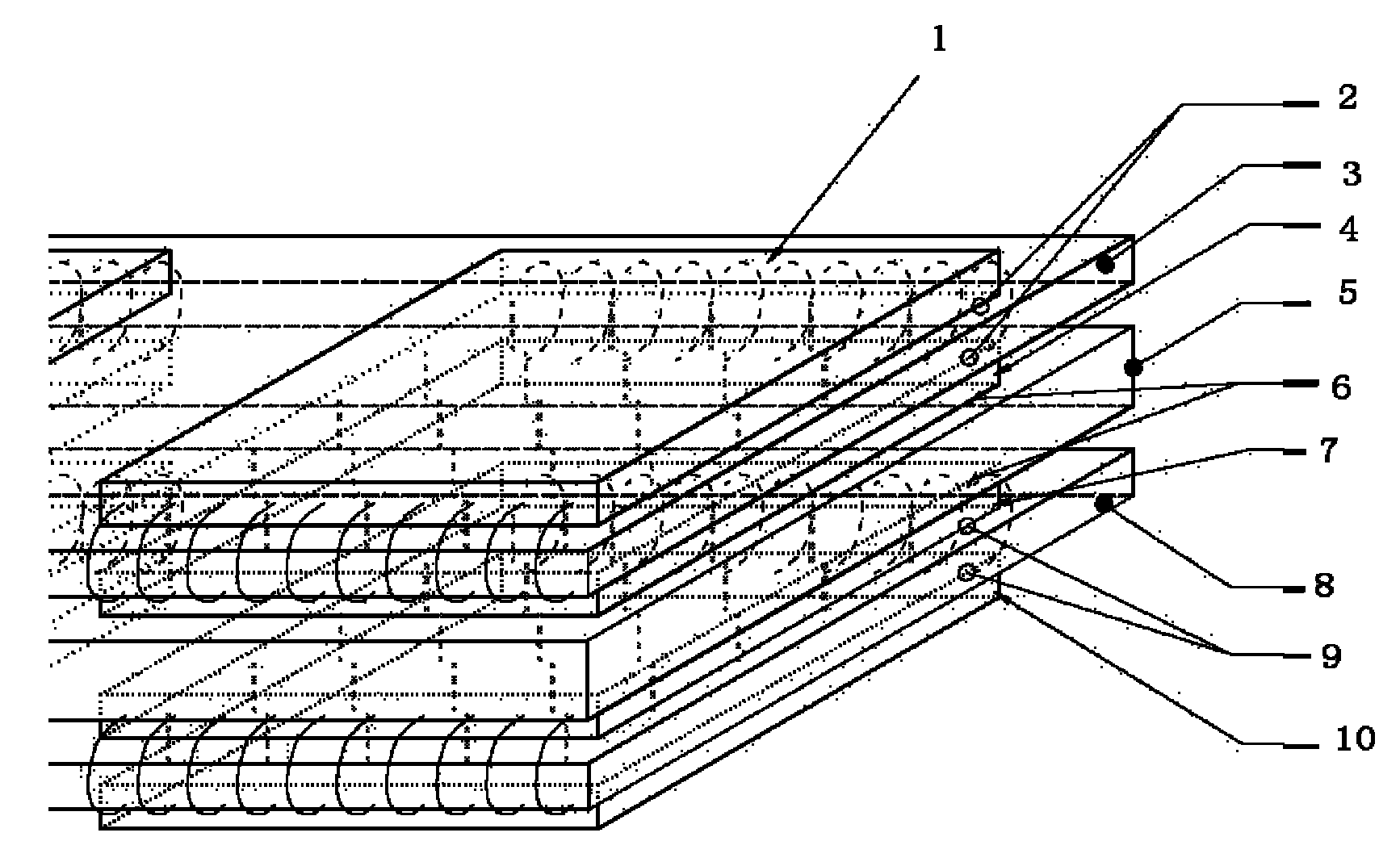
[0011] In the embodiment of the present invention, the method for integrating multi-layer multi-chip packaging on a multi-layer packaging circuit substrate and the package made by this method, the line distance and line width of the packaging circuit substrate are less than 20 microns, and a logic chip is stacked On top of the other, form the middle layer (core part) two identical chips stacked, and the upper layer (top) stack one large-capacity memory chip on top of the other to form the top two chips stacked on the core part chip, so that the upper layer and The middle layer is connected to the same symmetrical position with flexible circuit terminals. Four packaged chips are stacked to form a package for conductive connection to form a stacked layer. The four chips are packaged on a flexible circuit substrate with a total thickness of less than 1.20mm, realizing ball grid array packaging technology (FBGA) and Chip Scale Package (FCSP) package manufacturing.

[0012] In this...


PUM

PropertyMeasurementUnit
Diameteraaaaaaaaaa

Abstract

The invention relates to a method for packaging a multi-laminated multi-chip on a flexible circuit board by adopting FUTCP (Flexible Ultra-thin Three-dimensional Chip Package) and a packaging chipset. Two packaging chips are bound on a middle-layer (bottom) flexible circuit terminal, two packaging chips which are bound on the same symmetrical position of an upper-layer (top) flexible circuit terminal are mutually connected through ACAF (Anisotropic Conductive Adhesives and Films), the chips are stacked, mutually connected and packaged by using NCP (Non-conductive paste), and a chip stacking assembly is packaged by adopting a high-frequency LCP (Liquid Crystal Polymer) chip to bond the multilayer chip and simultaneously solidified; the edge bend of each packaging chip which is connected with the upper-layer (top) flexible circuit is connected with the two middle-layer (bottom) packaging chips in the packaging process so as to form a stacking layer, and the four chips are packaged on the flexible circuit board.

Description

technical field [0001] The invention relates to a multi-stacked multi-chip package, in which a plurality of chips are stacked on a flexible circuit substrate and integrated into a packaged chip group. Specifically, one chip is stacked on top of the other, high-density digital logic devices are integrated and packaged in the middle, and a large-capacity memory is stacked on the top, and conductive connections are made through flexible circuits. technical background [0002] Flexible ultra-thin chip three-dimensional packaging (FUTCP, Flexible ultra-thin chip package), also known as flexible three-dimensional electronic packaging technology, three-dimensional electronic packaging technology, is based on the X-Y plane two-dimensional packaging (referred to as COF packaging), to the three-dimensional direction ( The high-density electronic packaging technology developed by Z-axis) has smaller packaging volume, weight, delay, noise and power consumption, and higher speed and inte...

Claims


Application Information

Patent Timeline
IPC IPC(8): H01L21/50H01L21/60H01L25/18H01L23/498
CPCH01L2924/0002H01L2924/00
Inventor 刘萍
Owner SHENZHEN DANBOND TECH
Why Eureka
Try Eureka