Capacitive ultrasonic sensor and manufacturing method thereof

An ultrasonic sensor, capacitive technology, applied in the measurement of ultrasonic/sonic/infrasonic waves, instruments, electrical devices, etc., can solve the problems of difficult IC circuit integration, difficult metal connection, and easy process preparation. The effect of short production cycle and few process steps

Inactive Publication Date: 2015-05-27
INST OF SEMICONDUCTORS - CHINESE ACAD OF SCI
View PDF8 Cites 14 Cited by
  • Summary
  • Abstract
  • Description
  • Claims
  • Application Information

AI Technical Summary

Problems solved by technology

He Changde's research group at North University of China used anodic bonding to prepare capacitive ultrasonic sensors. However, during the process of anodic bonding, high-voltage treatment is required, and the preparation of capacitive ultrasonic sensors is prone to breakdown of the insulating layer, causing the diaphragm to collapse; Bonding technology with agent or metal as the intermediate medium, the process preparation is not difficult, but it is easy to introduce pollution such as adhesives and metal ions
Silicon wafer direct bonding technology can avoid the disadvantages of anodic bonding and bonding technology with adhesive as the intermediate medium, but the traditional silicon wafer direct bonding technology has a high annealing temperature (about 1000 ° C), and it is difficult to integrate with IC circuits Larger, difficult to achieve metal connection

Method used


Image

  • Capacitive ultrasonic sensor and manufacturing method thereof
  • Capacitive ultrasonic sensor and manufacturing method thereof
  • Capacitive ultrasonic sensor and manufacturing method thereof

Examples


Embodiment Construction

[0029] In order to make the object, technical solution and advantages of the present invention clearer, the present invention will be described in further detail below in conjunction with specific embodiments and with reference to the accompanying drawings.

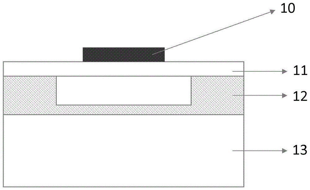
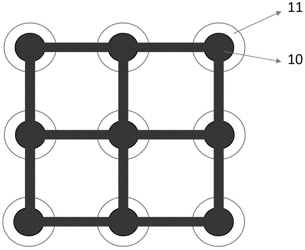
[0030] In the present invention, the capacitive ultrasonic sensor uses a low-resistance silicon substrate directly as the lower electrode, uses silicon dioxide as the insulating layer material, uses the top silicon of SOI as the diaphragm, and directly connects the SOI sheet and the silicon substrate with the cavity After bonding, the bottom silicon and buried oxide layer of SOI are etched away, and metal is deposited on the top silicon of SOI as the upper electrode, finally forming a capacitive ultrasonic sensor.

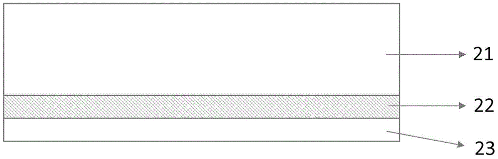
[0031] The invention is realized through the following technical solutions: based on the low-temperature silicon chip direct bonding technology, a capacitive ultrasonic sensor is prepared. The low-resistance s...


PUM

PropertyMeasurementUnit
electrical resistivityaaaaaaaaaa
thicknessaaaaaaaaaa

Abstract

The invention discloses a capacitive ultrasonic sensor. The capacitive ultrasonic sensor comprises a low-resistivity silicon substrate, a silicon oxide layer formed on the low-resistivity silicon substrate, a two-dimensional cavity array structure formed in the silicon oxide layer, a diaphragm formed above the two-dimensional cavity array structure and an upper electrode formed by deposition of metal aluminum on the diaphragm, wherein the upper electrode is a graph array, and graphs in the graph array of the upper electrode and the graphs in the two-dimensional cavity array structure are distributed in a one-to-one correspondence manner and mutually connected together. According to the capacitive ultrasonic sensor disclosed by the invention, wet process and dry process surface activation treatment is performed on the silicon substrate and an SOI (silicon-on-insulator) chip, a low-temperature silicon chip direct bonding technology is adopted, and the prepared capacitive ultrasonic sensor has the advantages of miniaturization, high reliability, good repeatability, relatively few process steps, short manufacturing period and the like; furthermore, the process temperature is relatively low, and the capacitive ultrasonic sensor is easy to be integrated with an IC (integrated circuit) for realizing integral packaging of the chip.

Description

technical field [0001] The invention relates to a capacitive ultrasonic sensor in the field of sensors, in particular to a capacitive ultrasonic sensor based on low-temperature silicon chip direct bonding technology and a manufacturing method thereof. Background technique [0002] Ultrasonic sensors are widely used in medical imaging, non-destructive testing, and ultrasonic microscopy. Broadband, multi-dimensional high density, and miniaturization are the main directions for the development of ultrasonic transducers in the future. In the past few decades, piezoelectric ultrasonic transducers based on piezoelectric materials have become the mainstream ultrasonic transducer devices, but in recent years, a capacitive ultrasonic sensor has gradually become one of the main research directions of ultrasonic transducers. Compared with the traditional piezoelectric ultrasonic transducer, the capacitive ultrasonic transducer has the following advantages: first, it adopts the manufac...

Claims


Application Information

Patent Timeline
Patent Type & Authority Applications(China)
IPC IPC(8): G01H11/06B81C1/00
Inventor 王小青孙英男宁瑾俞育德
Owner INST OF SEMICONDUCTORS - CHINESE ACAD OF SCI
Why Eureka
Try Eureka