Solder resist ink circuit board manufacture method

A production method and technology of solder resist ink, applied in the manufacture of printed circuits, applying paste/ink/powder resists, printed circuits, etc., can solve the problem of easily exceeding the thickness requirements of solder resist inks, failing to meet production needs, ink thickness, etc. Height difference and other problems, to achieve the effect of uniform thickness, high degree of automation and strong applicability

Active Publication Date: 2015-03-11
东莞康源电子有限公司
View PDF14 Cites 7 Cited by
  • Summary
  • Abstract
  • Description
  • Claims
  • Application Information

AI Technical Summary

Problems solved by technology

[0003] At present, the thickness tolerance of solder resist ink in the industry is usually plus or minus 10um. The above-mentioned screen printing does not process the ink on the board. Due to the height difference of the copper thickness at different positions on the board, it is easy to cause the thickness of the ink on the board. There is also a height difference, and it is easy to exceed the thickness requirements of the solder resist ink in the industry, which cannot meet the production needs

Method used


Image

  • Solder resist ink circuit board manufacture method

Examples


Embodiment Construction

[0020] In order to make the technical solution of the present invention more clearly expressed, the present invention will be further described below in conjunction with the accompanying drawings.

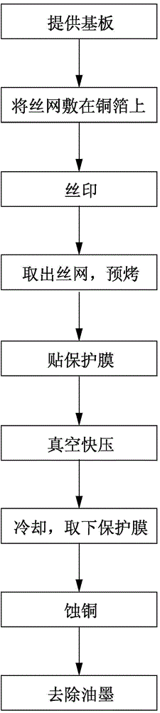
[0021] Such as figure 1 As shown, the present invention provides a kind of manufacture method of solder resist ink circuit board, comprises the following steps:

[0022] Step (1): providing a substrate, the substrate is provided with copper foil;

[0023] Step (2): Lay the screen on the copper foil of the substrate, the screen is provided with mesh holes, and the distribution of the mesh holes corresponds to the circuit pattern;

[0024] Step (3: silk screen printing, apply the ink on the screen, the ink flows from the mesh of the screen to the surface of the copper foil, forming an ink pattern on the surface of the copper foil, corresponding to the circuit pattern;

[0025] Step (4: Take out the screen, put the substrate into a baking machine, and pre-bake it so that the ink on ...


PUM


Abstract

A solder resist ink circuit board manufacture method includes providing a substrate, paving a screen on the copper foil of the substrate, painting ink on the screen, removing the screen, fitting a protecting film on the substrate, pressing rapidly in vacuum, cooling, removing the protecting film, performing copper etch, removing the copper foil except for the ink layer and removing the ink on the surface of the copper foil. According to the method, after the screen printing is adopted, the protecting film is fitted to the surface of the solder resist ink, the ink is pressed in the manner of vacuum rapid pressing, the thickness of the ink is even and is controlled, the thickness of the ink can be adjusted according to production requirements, the adaptability is high, the automation level is high, and the product qualification rate is guaranteed.

Description

technical field [0001] The invention relates to the technical field of circuit boards, in particular to a method for manufacturing circuit boards with solder resist ink. Background technique [0002] Screen printing has the advantages of thick ink layer, strong coverage, and is not limited by the surface shape of the substrate and the size of the area. It is widely used in the production of PCB boards. Printing is based on the basic principle that the ink is transparent, and the non-graphic part of the mesh is impermeable to ink. Pour ink into one end of the screen printing plate, apply a certain pressure on the ink part on the screen printing plate with a squeegee, and move towards the other end of the screen printing plate at the same time. The ink is squeezed by the scraper from the mesh of the graphic part to the substrate during the movement. [0003] At present, the thickness tolerance of solder resist ink in the industry is usually plus or minus 10um. The above-ment...

Claims


Application Information

Patent Timeline
Patent Type & Authority Applications(China)
IPC IPC(8): H05K3/28
CPCH05K3/284H05K2203/0568
Inventor 杜军黄朝津杨建勇
Owner 东莞康源电子有限公司
Why Eureka
Try Eureka