Disjunction method of semiconductor wafer

A semiconductor and wafer technology, applied in the field of semiconductor wafer cutting, can solve the problems of perfect cutting section, quality or yield reduction, intrusion, etc., to achieve the effect of effective use of materials

Active Publication Date: 2015-03-18
MITSUBOSHI DIAMOND IND CO LTD
View PDF7 Cites 0 Cited by
  • Summary
  • Abstract
  • Description
  • Claims
  • Application Information

AI Technical Summary

Problems solved by technology

[0009] However, in grooving by cutting with a rotary blade, a large amount of chips are generated, and even after cleaning with a cutting fluid, for example, a part of the cutting fluid may remain in the groove or on the surface where the groove is formed, or due to Scattering during cutting causes cutting chips to adhere to silicon wafers, etc., which is a major cause of quality and yield degradation
In addition, since a mechanism or piping is required for supplying cutting fluid or collecting waste fluid, the scale of the device becomes large.
In addition, since the grooving is performed by cutting, there may be small chips (defects) on the cutting surface or the edge of the groove, and it is impossible to obtain a perfect split surface
In addition, since the tip of the blade of the rotary blade rotating at high speed is formed in a sawtooth shape, abrasion or breakage of the tip of the blade is likely to occur and the service life is short.
Furthermore, since the thickness of the rotary blade cannot be made relatively thin in terms of strength, and even a small diameter one has a thickness of 60 μm or more, it is necessary to have a cutting width equivalent to the width of the blade, and it is also a limitation. Issues such as one of the factors for the effective use of materials
[0010] Further, in conventional procedures, such as Image 6 As shown, since the silicon wafer 13 is ground by the rough grinding stone 17, the groove 14 is penetrated and the fine grinding stone 18 is used for grinding again. Therefore, there is also the intrusion of grinding debris and the like from the penetrated groove 14. Protective sheet 16 side and remaining problem points

Method used


Image

  • Disjunction method of semiconductor wafer
  • Disjunction method of semiconductor wafer
  • Disjunction method of semiconductor wafer

Examples


Embodiment Construction

[0036] In order to further explain the technical means and effects adopted by the present invention to achieve the intended purpose of the invention, the specific implementation, structure, Features and their functions are described in detail below.

[0037] Hereinafter, details of the method for dividing a semiconductor wafer according to the present invention will be described with reference to the drawings.

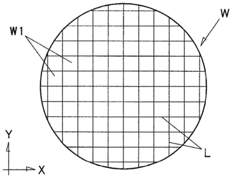
[0038] figure 1It is a plan view of a silicon wafer to be processed, and is divided along grid-like planned breaking lines L extending in the X-Y direction by the following breaking method to take out wafer-sized unit products W1. The silicon wafer W to be processed has a thickness of, for example, 100 to 300 μm before slicing, and is thinned to a thickness of 25 to 50 μm in a slicing process described below.

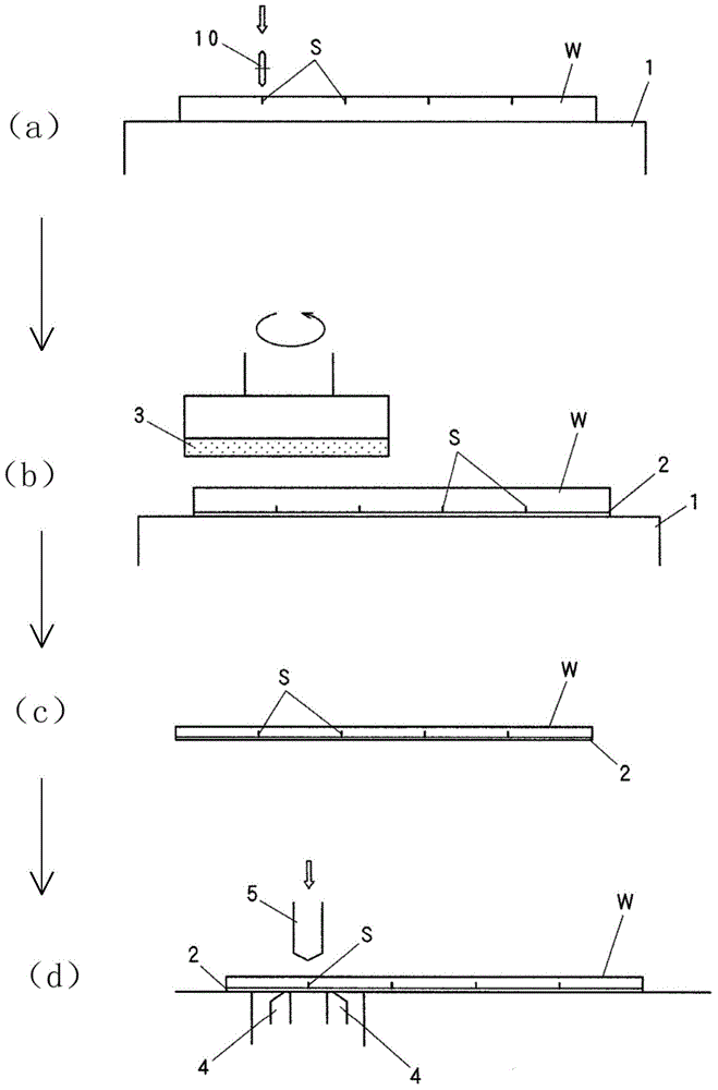
[0039] figure 2 An explanatory diagram showing an example of a method for breaking a silicon wafer (semiconductor wafer) W according to the present inventi...


PUM


Abstract

The invention relates to a disjunction method of a semiconductor wafer, which does not use a dicing saw, realizes effective and perfect disjunction by a simple technique, and can achieve a thin sheet. A scratching wheel (10) press while rotate along a disjunction predetermined line (L) to form a scratching line (S) formed by a crack penetrating in the thickness direction, and the depth of the crack is to the degree of not penetrating the whole range of the thickness of a semiconductor wafer (W) which is cut by a cut millstone (3) subsequently to become a thin sheet; then, the semiconductor wafer (W) is reversed, and the surface opposite to the surface provided with the scratching line (S) is cut by the cut millstone (3) to form a thin-sheet semiconductor wafer (W); next, the surface opposite to the surface provided with the scratching line (S) is pressed by a breaking rod (5) along the scratching line (S) to bend the semiconductor wafer (W), so as to enable the crack to further penetrate and thus to disjunct the semiconductor wafer (W).

Description

technical field [0001] The present invention relates to a method for dividing a semiconductor wafer such as silicon having electronic circuits formed on its surface, and more particularly relates to a method for dividing a plurality of electronic circuits formed along the surface of a semiconductor wafer as a parent body. A method of cutting a semiconductor wafer into wafer-sized unit products by cutting on a predetermined line for breaking. Background technique [0002] Silicon wafers used in the manufacture of various semiconductor elements are required to be thinner from the standpoint of low power consumption and higher integration. Recently, thinner thicknesses have been required to be as low as 25 μm to 50 μm. . Thinning of a silicon wafer is generally performed by grinding the surface opposite to the surface on which the electronic circuit is formed with a flat grinding stone. However, once the thickness is reduced, distortion occurs due to the influence of residual...

Claims


Application Information

Patent Timeline
Patent Type & Authority Applications(China)
IPC IPC(8): H01L21/304
CPCH01L21/3043H01L21/67092
Inventor 上村刚博
Owner MITSUBOSHI DIAMOND IND CO LTD
Why Eureka
Try Eureka