

Snubber circuit and buffering method for snubber circuit
A snubber circuit and discharge current technology, which is applied in the snubber field of snubber circuits, can solve problems such as reducing power conversion efficiency and increasing energy loss, and achieves the effect of eliminating power loss and long reverse current recovery time
- Summary
- Abstract
- Description
- Claims
- Application Information
AI Technical Summary
Problems solved by technology
Method used
Image

Examples
Embodiment Construction
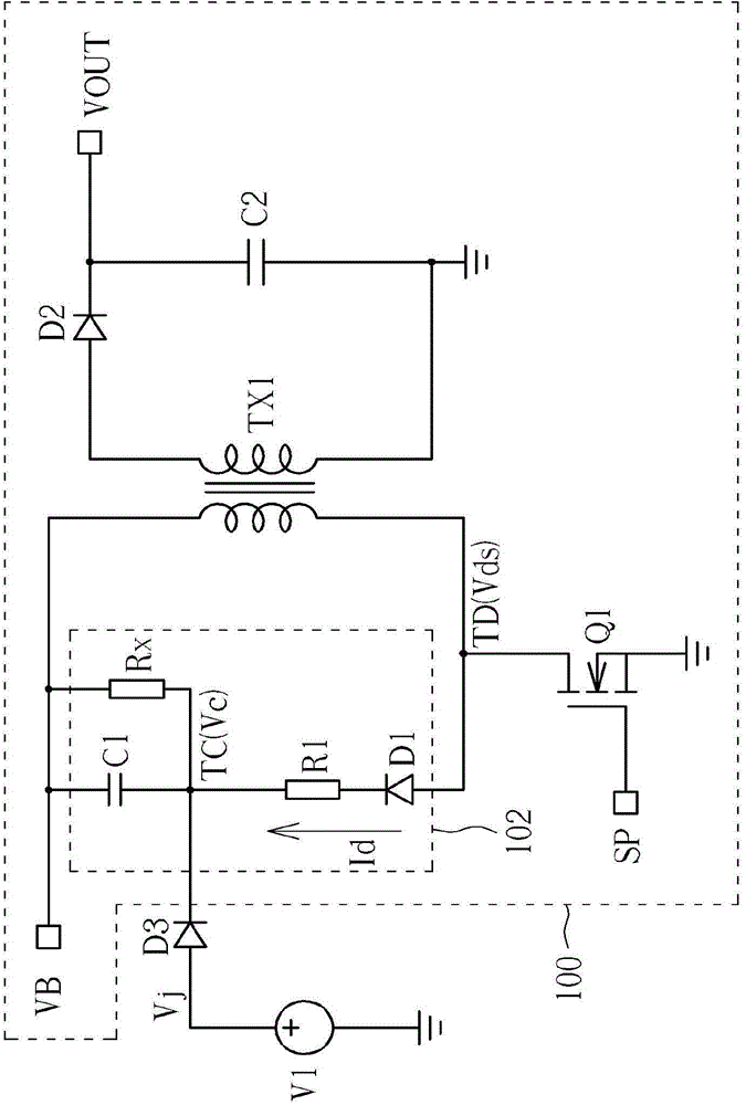
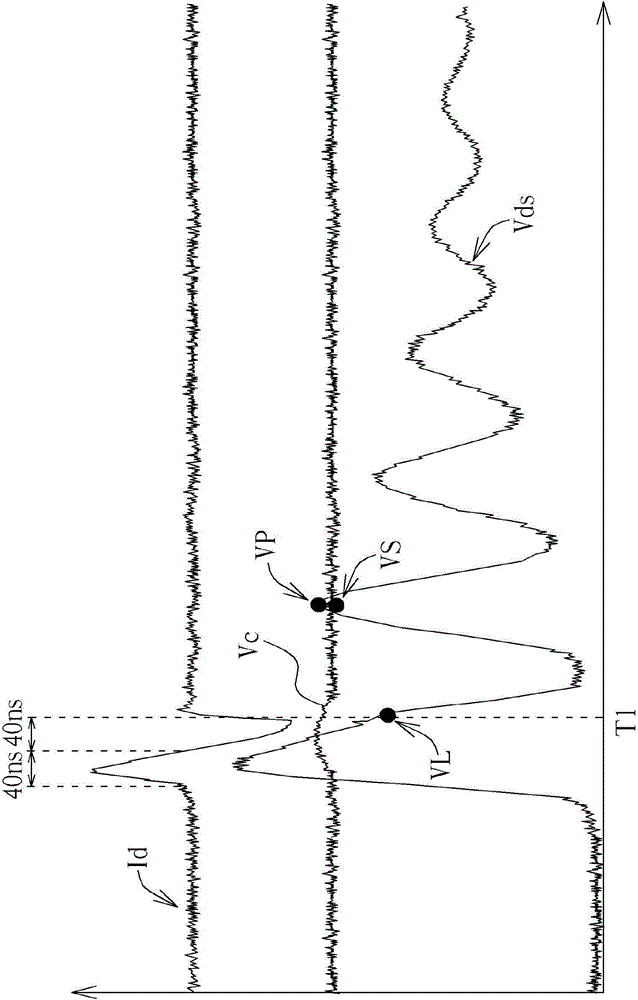
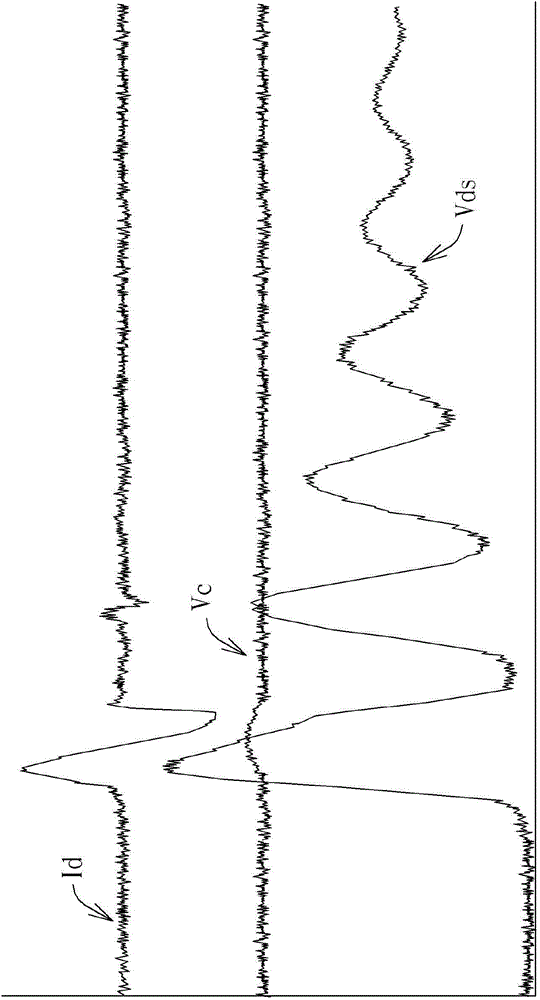
[0074] In order to realize a snubber circuit that can be applied to high-speed switching and has low energy loss, the present invention first tests the existing snubber circuit to analyze the circuit characteristics of the existing snubber circuit, and discloses a snubber circuit according to the test results. buffer device. Further explanation follows.
[0075] see again figure 1 , which also shows a schematic diagram of an embodiment of the circuit structure used to test the existing buffer circuit of the present invention. Depend on figure 1 It can be seen that the RCD snubber circuit 102 is disposed on the primary side of the DC-to-DC converter 100 including the transformer TX1 , the switch Q1 , the diode D2 and the capacitor C2 . Those skilled in the art should be able to understand the details of the operation of the DC-DC converter 100 to convert an input voltage VB into an output voltage VOUT according to a control signal SP (for example, a pulse width modulation (P...
PUM
 Abstract
Description
Claims
Application Information