Touch substrate and touch device

A substrate and touch technology, applied in optics, instruments, electrical and digital data processing, etc., can solve the problem of no technical support for incelltouch touch screens, and achieve the goal of improving product market competitiveness, reducing matching difficulty, and reducing node capacitance. Effect

Inactive Publication Date: 2015-03-25
BOE TECH GRP CO LTD +1
View PDF6 Cites 14 Cited by
  • Summary
  • Abstract
  • Description
  • Claims
  • Application Information

AI Technical Summary

Problems solved by technology

[0003] At present, there is a trend of combining ADS technology with in cell touch technology, but on the issue of how to reduce the node coupling capacitance between touch electrodes, the current in cell touch screen has not yet appeared. technical support

Method used


Image

  • Touch substrate and touch device
  • Touch substrate and touch device
  • Touch substrate and touch device

Examples


Embodiment Construction

[0027] The following will take a liquid crystal display device with a touch function as an example, and introduce the touch substrate and the touch device provided in the embodiments of the present invention with reference to the accompanying drawings.

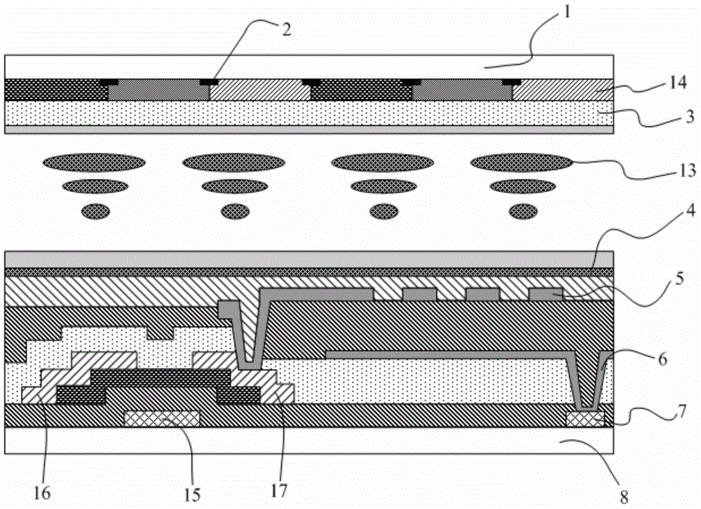
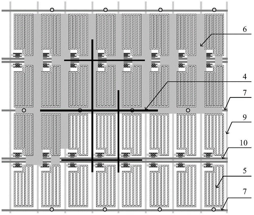
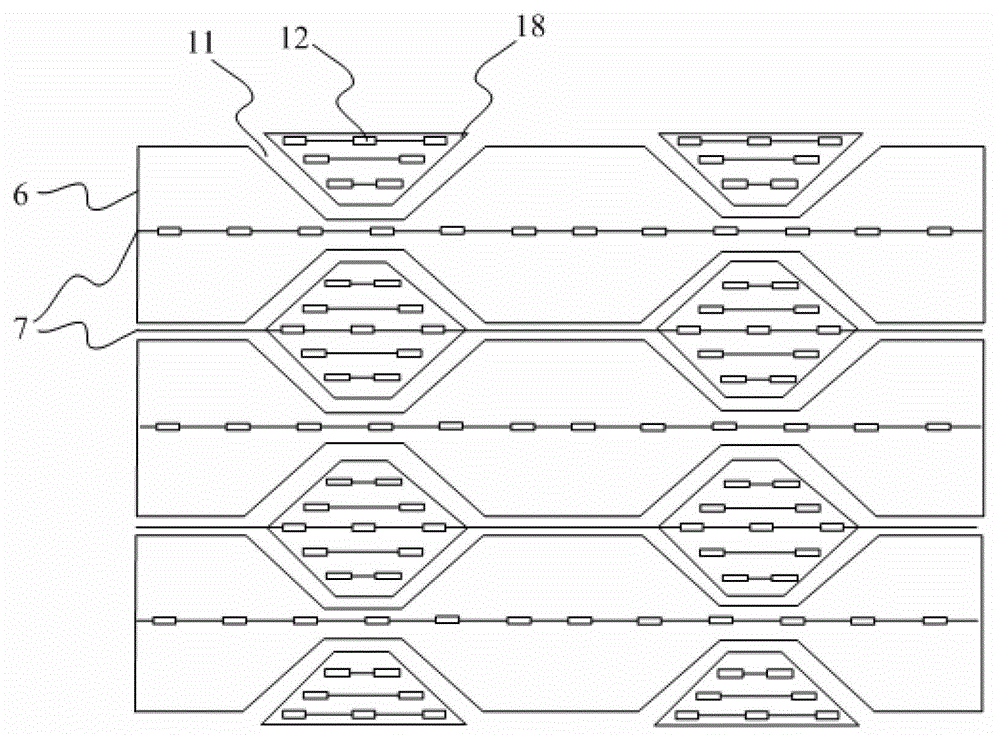
[0028] combine figure 1 and Figure 4 As shown, the touch substrate provided by the embodiment of the present invention includes a thin film transistor, and a transparent common electrode layer and a pixel electrode layer; wherein, the common electrode layer includes a common electrode 18 and a touch driving electrode extending along the first direction 6. An insulating medium is filled between the common electrode 18 and the touch driving electrode 6;

[0029] The touch control substrate is also provided with a touch sensing electrode 4 arranged in a different layer from the touch driving electrode 6 and extending along the second direction. The touch sensing electrode 4 covers the gap between the common electrode and the to...


PUM


Abstract

The embodiment of the invention discloses a touch substrate and a touch device. The touch substrate comprises a thin film transistor, a transparent public electrode layer and a pixel electrode layer. The public electrode layer comprises public electrodes and touch drive electrodes, wherein the public electrodes and the drive electrodes extend in a first direction, and space between the public electrodes and the touch drive electrodes is filled with insulation dielectric; the touch substrate is further provided with touch sensing electrodes, wherein the touch sensing electrodes are at different layers from the touch drive electrodes and extend in a second direction, and the space between the public electrodes and the touch drive electrodes is covered with the touch sensing electrodes; within the display time of a frame of image, the touch drive electrodes are used for transmitting public electrode signals and touch scanning signals in a time-share mode. The touch drive electrodes and the touch sensing electrodes do not have alignment areas, the node capacitance of touch electrodes can be reduced to the maximal extent, and the touch sensitivity is improved.

Description

technical field [0001] The invention relates to the field of touch technology, in particular to a touch substrate and a touch device. Background technique [0002] At present, the display technologies that can realize wide viewing angle mainly include IPS technology (In-Plane Switch, in-plane switching technology) and ADSDS (ADvanced Super Dimension Switch, advanced super dimension field switching technology, referred to as ADS); among them, ADS technology is mainly through the same The electric field generated by the edge of the slit electrode in the plane and the electric field generated between the slit electrode layer and the plate electrode layer form a multidimensional electric field, so that all oriented liquid crystal molecules between the slit electrodes in the liquid crystal cell and directly above the electrodes can be rotated, thereby The working efficiency of the liquid crystal is improved and the light transmission efficiency is increased. Advanced ultra-dimen...

Claims


Application Information

Patent Timeline
Patent Type & Authority Applications(China)
IPC IPC(8): G06F3/041G06F3/044
CPCG06F3/044G02F1/134363G02F1/13338G02F2201/121G02F2201/123G06F3/0412G06F3/0445G06F3/0446G06F3/0443G02F1/134372H10K59/40G02F1/133512G02F1/133514G02F1/1341G02F1/134309G02F1/13439G02F1/136286G02F1/1368G06F3/045G06F2203/04111
Inventor 杨盛际
Owner BOE TECH GRP CO LTD
Why Eureka
Try Eureka