

A pressing and fixing component for packaging transistors
Patent Information
- Authority / Receiving Office
- CN · China
- Patent Type
- Patents(China)
- Current Assignee / Owner
- GOODWE TECHNOLOGIES CO LTD
- Publication Date
- 2017-09-05
Smart Images
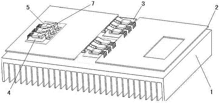
Figure 1 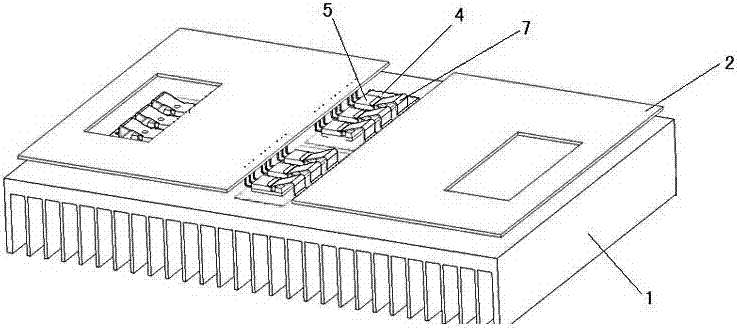
Figure 2 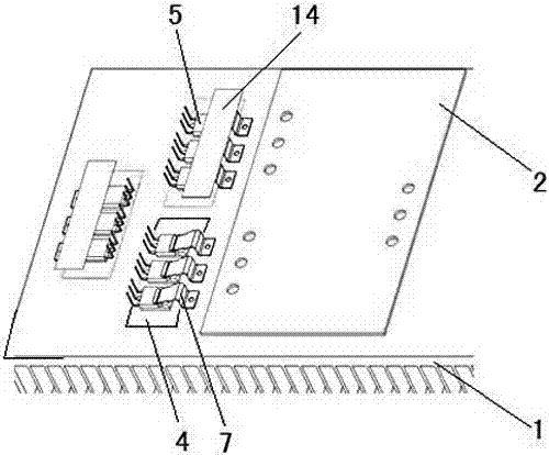
Figure 3
Abstract
Description
technical field
[0001] The invention belongs to the technical field of switching power supplies and photovoltaic inverters, and is applied to the T0247 packaging used in current AC-DC conversion or similarly packaged transistors for heat dissipation, pressing and fixing, and specifically relates to a pressing and fixing assembly for packaging transistors. Background technique
[0002] At present, in the field of photovoltaic inverters, there are mainly the following methods for the assembly, heat dissipation, compression and fixing of transistors and PCBA boards:
[0003] 1. PCBA opening, transistor mounting, wave soldering, such as figure 1 As shown, for this structure, the machine welding of the transistor 5 has certain advantages in consistency, quality and cost, but it is necessary to increase the intermediate transition heat sink 3, so that the heat conduction resistance increases, and the heat dissipation performance of the transistor 5 decreases. In addition, the PCBA...