A semiconductor switch chip and its manufacturing method

A switching chip and manufacturing method technology, applied in semiconductor/solid-state device manufacturing, semiconductor devices, electronic switches, etc., can solve the problems of high manufacturing cost, high power consumption of switching power supply, and susceptibility to electromagnetic interference, and achieve accurate temperature detection, Reduce static power consumption, require simple effects

Active Publication Date: 2017-06-09
FOUNDER MICROELECTRONICS INT
View PDF4 Cites 0 Cited by
  • Summary
  • Abstract
  • Description
  • Claims
  • Application Information

AI Technical Summary

Problems solved by technology

[0011] The invention provides a semiconductor switch chip and its manufacturing method to solve the problems of high power consumption, high manufacturing cost and susceptibility to electromagnetic interference in the existing switching power supply

Method used


Image

  • A semiconductor switch chip and its manufacturing method

Examples


Embodiment 1

[0048] This embodiment provides a semiconductor switch chip, which is used in semiconductor devices, such as communication equipment, mobile equipment, industrial equipment, household appliances, personal computers, and the like. More precisely, it is applied to semiconductor chips and their manufacturing processes. Semiconductor switch chip of the present invention comprises:

[0049] a switching device, used for pulse modulation of the input voltage; the switching device includes a first lateral double-diffused MOS transistor;

[0050] A high-voltage starting device is used to turn on the control chip on the periphery of the semiconductor switch chip, and the control chip is used to turn on and off the switching device; the high-voltage starting device includes a second lateral double-diffused MOS transistor, a voltage regulator Diodes and high-value resistors;

[0051] A temperature detection device is used to detect the temperature of the switching device in real time. ...

Embodiment 2

[0057] This embodiment and Embodiment 1 belong to the same inventive concept. This embodiment provides a method for manufacturing a semiconductor switch chip, including the following steps:

[0058] S1: generating a switching device, the switching device is used for pulse modulation of the input voltage; the switching device includes a first lateral double-diffused MOS transistor;

[0059] S2: Generate a high-voltage starting device, the high-voltage starting device is used to turn on the control chip on the periphery of the semiconductor switch chip, and the control chip is used to realize the function of turning on and off the switching device; the high-voltage starting device includes a second lateral double Diffused MOS transistors, Zener diodes and high resistance resistors;

[0060] S3: generating a temperature detection device, which is used to detect the temperature of the switching device in real time.

[0061] As can be seen from the above description, the temperat...

Embodiment 3

[0080] The present invention is described below through an actual scene.

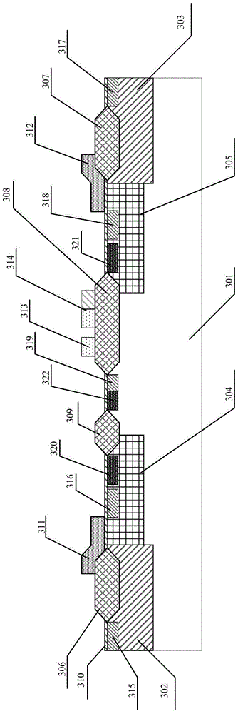
[0081] The semiconductor switch chip of this embodiment includes at least two LDMOS, a bulk silicon diode, a polysilicon voltage regulator diode, and a polysilicon high-resistance resistor. These elements are integrated in the same chip and connected with metal according to functional requirements; One LDMOS is connected with the polysilicon voltage regulator diode and the polysilicon high-resistance resistor to realize the high-voltage start-up function, and the other LDMOS is used as a switching device; the body silicon diode realizes the temperature detection function; thereby realizing the high-voltage start-up function LDMOS switching device with temperature detection function;

[0082]Wherein, the bulk silicon diode is composed of N-type doped silicon and P-type doped silicon, and the doping concentration of N-type doped silicon and P-type doped silicon is not limited; the polysilicon high resista...


PUM


Abstract

The invention discloses a semiconductor switch chip and a manufacturing method thereof in the technical field of semiconductor chips and manufacturing techniques thereof. The present invention includes a switching device, used for pulse modulation of the input voltage; the switching device includes a first lateral double-diffused MOS transistor; a high-voltage starting device, used for turning on the control chip on the periphery of the semiconductor switch chip, and the control chip uses The switching device is used to turn on and off; the high-voltage starting device includes a second lateral double-diffused MOS transistor, a Zener diode and a high-resistance resistor; a temperature detection device is used to detect the temperature of the switching device in real time. The invention is not disturbed by external environmental factors, and can detect the temperature change of the switching device very sensitively; the switching device and the high-voltage starting device are integrated in the same chip, which can improve the starting efficiency and reduce the static power consumption.

Description

technical field [0001] The invention relates to the technical field of a semiconductor chip and its manufacturing process, in particular to a semiconductor switch chip and its manufacturing method. Background technique [0002] Double diffused metal oxide transistor (DMOS) is one of the most common semiconductor devices. Its main function is to be used as a switching chip in switching power supplies (SMPS) of various equipment and facilities, such as communication equipment, mobile equipment, industrial equipment, household Electrical appliances, personal computers, etc. In the switching power supply, in addition to the switching chip, another important component is the control chip, that is, through the control chip, the switching chip is continuously "on" and "off", so that the switching chip performs pulse modulation on the input voltage. So as to realize AC-DC conversion, DC-DC conversion, automatic voltage stabilization and other functions. [0003] Double-diffused me...

Claims


Application Information

Patent Timeline
Patent Type & Authority Patents(China)
IPC IPC(8): H01L27/02H01L27/06H01L21/822H03K17/56
Inventor 潘光燃石金成文燕马万里高振杰
Owner FOUNDER MICROELECTRONICS INT
Why Eureka
Try Eureka