Integrated LED packaging structure

A packaging structure and LED chip technology, which is applied in lighting devices, electric solid-state devices, semiconductor devices, etc., can solve problems such as poor reliability, increased product volume, and reduced power supply life, achieving high space and degrees of freedom, increasing heat dissipation channels, The effect of improving product life

Inactive Publication Date: 2015-03-25
SHENZHEN JINGTAI
View PDF3 Cites 10 Cited by
  • Summary
  • Abstract
  • Description
  • Claims
  • Application Information

AI Technical Summary

Problems solved by technology

The existing SMD LED packaging mainly adopts the packaging form of metal ceramic substrate, PPA and metal wire bonding chip. Although PPA material has good thermal conductivity, it is easy to yellow and age; it has strong water absorption and poor metal bonding. After bonding with metal wires, due to the difference in expansion coefficient between the encapsulating gel and the metal wires during product use, there is a risk of breaking the bonding wires, resulting in poor reliability.
Traditional light sources mount SMD LEDs on metal-ceramic substrates and use external isolated or non-isolated power supplies. The separation of power supplies and light sources not only increases the size of the product, but also increases the design difficulty of the heat dissipation module, which makes the heat dissipation of the power supply difficult. To ensure that the life of the power supply is reduced and the life of the LED product is reduced

Method used


Image

  • Integrated LED packaging structure

Examples


Embodiment Construction

[0019] The following will clearly and completely describe the technical solutions in the embodiments of the present invention with reference to the accompanying drawings in the embodiments of the present invention. Obviously, the described embodiments are only some, not all, embodiments of the present invention. Based on the embodiments of the present invention, all other embodiments obtained by persons of ordinary skill in the art without making creative efforts belong to the protection scope of the present invention.

[0020] The embodiment of the invention discloses an integrated LED packaging structure with the characteristics of high production efficiency, good reliability and long life.

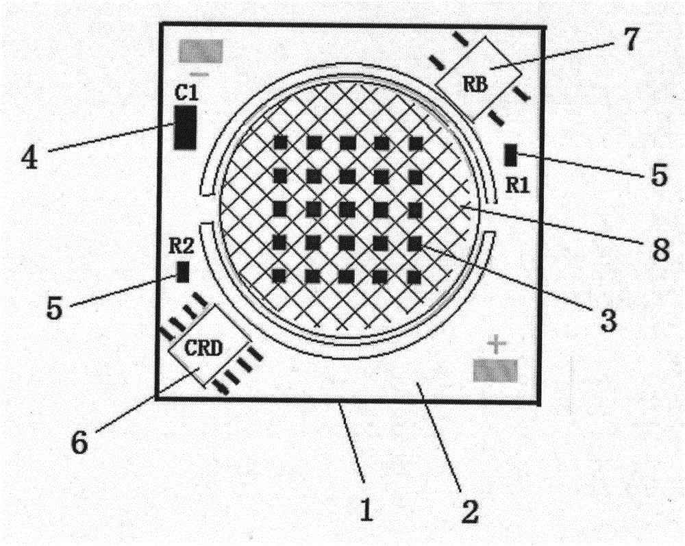
[0021] Please refer to the attached figure 1 , is a structural schematic diagram of an integrated LED packaging structure disclosed in the present invention, specifically including:

[0022] The ceramic substrate 1; the ceramic substrate 1 has positive and negative electrodes; an insul...


PUM


Abstract

The invention discloses an integrated LED packaging structure. The integrated LED packaging structure is characterized by comprising a ceramic substrate, an insulating layer covering the ceramic substrate, an inverted LED chip arranged on the ceramic substrate, a chip capacitor, a chip resistor, a current regulative diode, a rectifier and packaging glue covering the inverted LED chip, wherein the ceramic substrate is provided with a positive electrode and a negative electrode, and the chip capacitor, the chip resistor, the current regulative diode and the rectifier are arranged on the ceramic substrate. The chip capacitor, the chip resistor, the current regulative diode and the rectifier are collectively known as driving ICs. According to the integrated LED packaging structure, the inverted LED chip and the ceramic substrate with matched coefficients of expansion are adopted, the design of gold wires does not exist, the phenomenon that the packaging glue influences the product reliability when the packaging glue is expanded due to cold and heat changes is avoided, meanwhile, the driving ICs and the inverted LED chip share the ceramic substrate, a radiating channel of a power driving module is added, the product size is reduced, large space and the higher degree of freedom are provided for the design of the radiating module, the product working temperature is lowered, and the product service life is prolonged.

Description

technical field [0001] The invention relates to the technical field of LEDs, and more specifically relates to an integrated LED packaging structure. Background technique [0002] As the fourth generation of green lighting source, LED has been widely used. The existing SMD LED packaging mainly adopts the packaging form of cermet substrate, PPA and metal wire bonding chip. Although PPA material has good thermal conductivity, it is easy to yellow and age; it has strong water absorption and poor metal bonding. After bonding with metal wires, due to the difference in expansion coefficient between the packaging colloid and the metal wires during product use, there is a risk of breaking the bonding wires, resulting in poor reliability. Traditional light sources mount SMD LEDs on metal-ceramic substrates and use external isolated or non-isolated power supplies. The separation of power supplies and light sources not only increases the size of the product, but also increases the desi...

Claims


Application Information

Patent Timeline
Patent Type & Authority Applications(China)
IPC IPC(8): H01L33/48H01L33/64H01L25/00H05B37/02
CPCH01L25/16H01L33/48H01L33/642H05B47/10
Inventor 龚文邵鹏睿刘猛
Owner SHENZHEN JINGTAI
Why Eureka
Try Eureka