Method and system for repairing array substrate

An array substrate and metal layer technology, applied in the field of array substrate repair method and its system, can solve problems such as poor contact of TFT, difficult bridge connection, repair failure, etc.

Active Publication Date: 2015-04-08
CHENGDU VISTAR OPTEOLECTRONICS CO LTD
View PDF6 Cites 6 Cited by
  • Summary
  • Abstract
  • Description
  • Claims
  • Application Information

AI Technical Summary

Problems solved by technology

However, the process of forming a TFT array substrate is relatively complicated and cumbersome. In the complex process, TFT defects are often generated, and these defects include: short circuits, open circuits and other defects in the metal layer.
However, with the continuous development of TFT-LCD towards high resolution and high precision, TFT is getting thinner and thinner, and the area of ​​TFT is getting smaller and smaller. Using bridge connection will become a very difficult method.
When laser CVD is used to repair TFT defects, the thickness of the metal repair layer deposited on the substrate is difficult to monitor and control, and it is easy to cause poor contact of TFT after repair, resulting in repair failure

Method used


Image

  • Method and system for repairing array substrate
  • Method and system for repairing array substrate
  • Method and system for repairing array substrate

Examples


Embodiment Construction

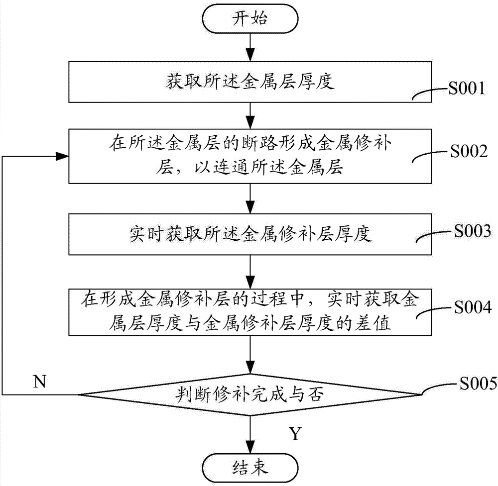
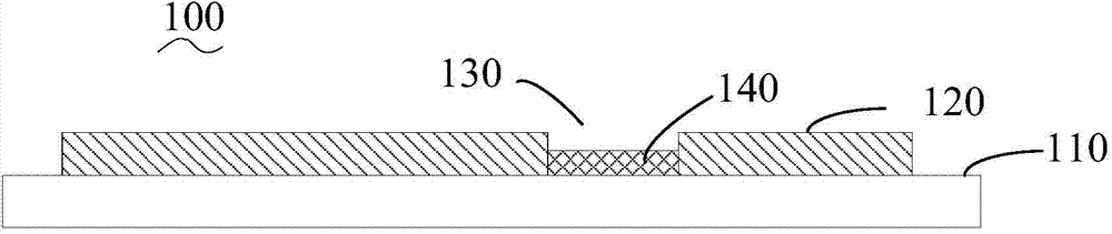
[0021] Please refer to figure 1 and figure 2 , figure 1 A flow chart of a method for repairing an array substrate, figure 2 Schematic diagram of an array substrate repaired for the array substrate repair method. The array substrate 100 includes a metal layer 120 , and there is an open circuit 130 between the metal layers 120 . The open circuit 130 may be an open circuit of a certain deposition layer of the metal layer 120 or a disconnection of several deposition layers or a fault in a metal layer. The method for repairing the array substrate comprises the following steps:

[0022] S001: Obtain the thickness of the metal layer 120 .

[0023] Acquisition of the thickness of the metal layer 120 , the thickness of the metal layer 120 obtained here is the thickness of the non-disconnected part of the metal layer 120 . In this embodiment, a thickness measurement device is used to measure the thickness of the metal layer 120 . In this embodiment, the thickness of the metal la...


PUM


Abstract

The invention discloses a method and a system for repairing an array substrate. The method includes forming a metal repairing layer in an open circuit of a metal layer on the array substrate to be communicated with the metal layer; in the process of forming the metal repairing layer, acquiring a difference value between thickness of the metal layer and that of the metal repairing layer in realtime; comparing the difference value with a preset threshold value, and when the difference value is smaller than or equal to the threshold value, completing repair. The system comprises a repairing device and a measuring device. According to the method, whether repairing is completed or not is judged by monitoring the difference value between the thickness of the metal layer and that of the metal repairing layer in realtime, so that film forming thickness of the metal repairing layer is monitored in realtime, completion of repairing is guaranteed to prevent bad contact after an TFT (thin film transistor) array is repaired, and repairing success rate is increased.

Description

technical field [0001] The invention relates to the field of flat display, in particular to a method and system for repairing an array substrate. Background technique [0002] Thin Film Transistor Liquid Crystal Display (TFT-LCD) is a kind of active matrix liquid crystal display (Active Matrix LCD). It has the characteristics of low power consumption, light and thin, easy to use, high brightness, high contrast, high response speed, and no radiation. It has become one of the mainstream technologies in the flat panel display industry. TFT array substrate is the key structure of TFT-LCD, so the quality of TFT array substrate is very important to the quality of TFT-LCD. However, the manufacturing process for forming the TFT array substrate is relatively complicated and cumbersome. In the complicated process, defects of the TFT are often generated, and these defects include defects such as short circuit and open circuit of the metal layer. [0003] In the prior art, laser chemi...

Claims


Application Information

Patent Timeline
Patent Type & Authority Applications(China)
IPC IPC(8): G02F1/13G02F1/1362H01L21/66
CPCG02F1/1309G02F1/136259H01L22/12
Inventor 杨旸胡贤夫马鹏程黄星星
Owner CHENGDU VISTAR OPTEOLECTRONICS CO LTD
Why Eureka
Try Eureka