Supercharge Your Innovation With Domain-Expert AI Agents!

Rram cell structure with laterally offset beva/teva

A technology of lateral offset and gate structure, applied in electrical components, semiconductor devices, circuits, etc., can solve problems such as high contact resistance change rate

Active Publication Date: 2015-04-15
TAIWAN SEMICON MFG CO LTD
View PDF5 Cites 7 Cited by
  • Summary
  • Abstract
  • Description
  • Claims
  • Application Information

AI Technical Summary

Problems solved by technology

However, conventional RRAM cells are capable of inducing a high rate of change in contact resistance at the top electrode via

Method used


Image

  • Rram cell structure with laterally offset beva/teva
  • Rram cell structure with laterally offset beva/teva
  • Rram cell structure with laterally offset beva/teva

Examples


Embodiment Construction

[0044] The description herein is made with reference to the drawings, wherein like reference numerals are generally used to refer to like elements throughout and the different structures are not necessarily drawn to scale. In the following description, for the purpose of illustration, numerous specific explanations are given for understanding. However, it will be apparent to those skilled in the art that one or more aspects herein may be practiced with a lesser degree of this detailed description. In other instances, well-known structures and devices are shown in block diagram form to facilitate understanding.

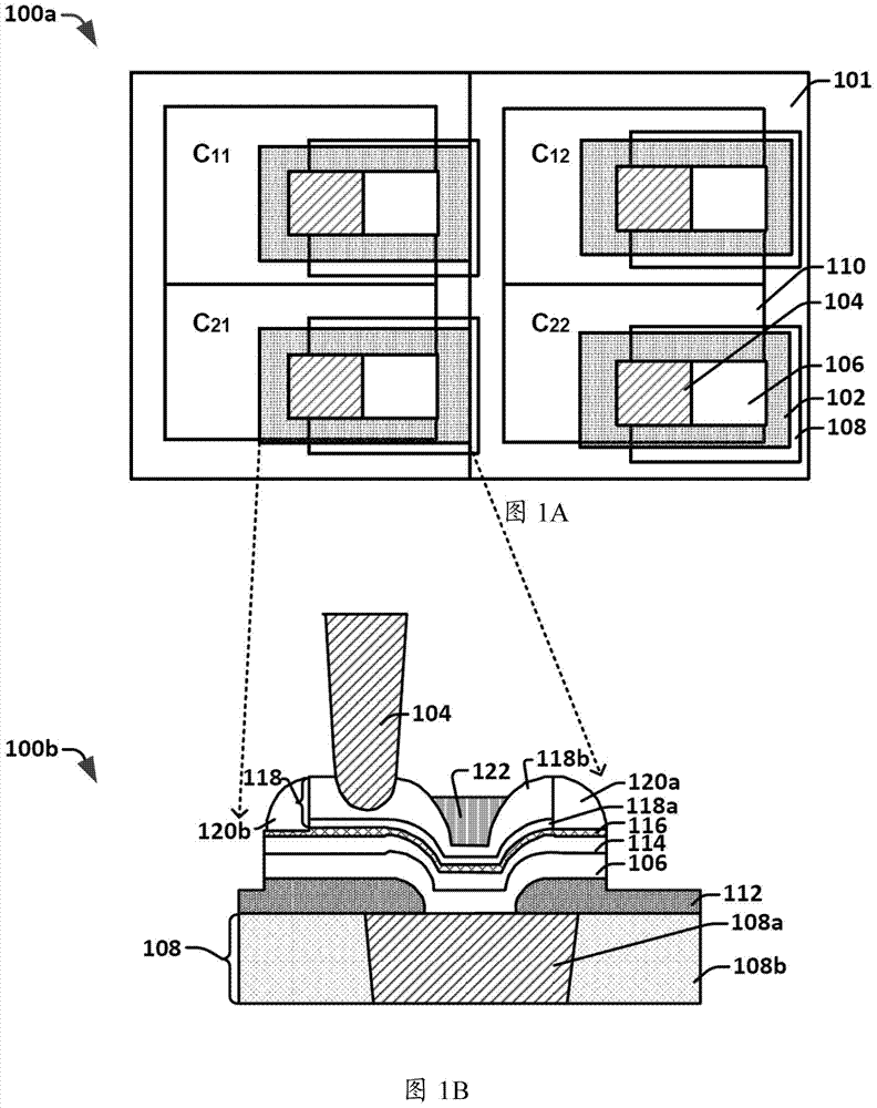
[0045]An RRAM cell includes two electrodes with a resistive switching element disposed between the two electrodes. The resistive switching element or variable resistive dielectric layer is prepared using a "forming process" to prepare the memory device for use. Typically the forming process is applied in a factory, assembly or initial system configuration. Resistive...


PUM


Abstract

The present disclosure relates to a resistive random access memory (RRAM) cell architecture, with off-axis or laterally offset top electrode via (TEVA) and bottom electrode via (BEVA). Traditional RRAM cells having a TEVA and BEVA that are on-axis can cause high contact resistance variations. The off-axis TEVA and BEVA in the current disclosure pushes the TEVA away from the insulating layer over the RRAM cell, which can improve the contact resistance variations. The present disclosure also relates to a memory device having a rectangular shaped RRAM cell having a larger area that can lower the forming voltage and improve data retention.

Description

technical field [0001] The present invention relates to the field of semiconductor technology, and more particularly, relates to a BEVA / TEVA RRAM cell structure with lateral offset. Background technique [0002] Nonvolatile memory is used in a wide variety of commercial and military electronics and equipment. Embedded flash memory devices are used to store data and executable programs in integrated chips. As the functionality of integrated chips increases, so does the need for greater memory capacity, forcing integrated chip designers and manufacturers to increase the available memory capacity while reducing the size and power consumption of the integrated chip. To achieve this goal, the size of memory cell components has been significantly reduced over the past few decades. Integrating floating gates and high-k metal gates becomes complex and expensive for embedded flash memory storage due to process technology shifts to smaller cell sizes. Resistive Random Access Memory...

Claims


Application Information

Patent Timeline
IPC IPC(8): H01L45/00
CPCH01L45/1675H01L45/1266H01L45/145H01L45/16H01L45/147H01L45/065H01L45/1691H01L45/1641H01L45/1608H01L45/124H01L45/1666H01L45/14H01L45/12H01L45/141H01L45/1625H01L45/149H01L45/1253H01L45/165H01L45/146H01L45/10H01L45/085H01L45/1293H01L45/1616H01L45/143H01L45/1246H01L45/1633H01L45/1213H01L45/08H01L45/1683H01L45/126H01L45/1273H01L45/148H01L45/122H01L45/1206H01L45/144H01L45/06H01L45/142H01L45/1286H01L45/1658H01L45/1226H01L45/04H01L45/1233H10B63/30H10N70/20H10N70/826H10N70/8833H10N70/063H10B53/30H10N70/8265H10N70/011H10N70/24H10N70/066H10N70/841H10N70/021H10N70/023H10N70/25H10N70/026H10N70/028H10N70/041H10N70/043H10N70/046H10N70/061H10N70/068H10N70/231H10N70/235H10N70/245H10N70/253H10N70/257H10N70/801H10N70/821H10N70/823H10N70/828H10N70/881H10N70/882H10N70/883H10N70/884H10N70/8413H10N70/8416H10N70/8418H10N70/8613H10N70/8616H10N70/8822H10N70/8825H10N70/8828H10N70/8836H10N70/8845
Inventor 张至扬朱文定涂国基廖鈺文陈侠威杨晋杰石昇弘游文俊
Owner TAIWAN SEMICON MFG CO LTD
Features
  • R&D
  • Intellectual Property
  • Life Sciences
  • Materials
  • Tech Scout
  • Unparalleled Data Quality
  • Higher Quality Content
  • 60% Fewer Hallucinations
Learn More