An apparatus, method and application for transfer of ultra-thin and flexible electronic devices

A technology for electronic devices and transfer devices, which is applied in the manufacture of electrical components, semiconductor/solid-state devices, circuits, etc., can solve the problems of being unable to meet the needs of rapid transfer of electronic devices, high requirements for preparation technology, and complicated manufacturing and forming processes. The effect of good reliability, high process reliability and simple control method

Active Publication Date: 2017-09-12
HUAZHONG UNIV OF SCI & TECH
View PDF9 Cites 1 Cited by
  • Summary
  • Abstract
  • Description
  • Claims
  • Application Information

AI Technical Summary

Problems solved by technology

However, this multi-layer microstructure still needs to rely on the relaxation characteristics of PDMs itself. The corner design and special laminated structure can accelerate the relaxation of the adhesive force, but the jacking time still depends on the characteristics of the material itself, and there is still chip debonding. The time is relatively long, and it cannot meet the current demand for rapid transfer of electronic devices, and the microstructure in it is complicated in the manufacturing and forming process due to its special structure, and has high requirements for the preparation process.

Method used


Image

  • An apparatus, method and application for transfer of ultra-thin and flexible electronic devices
  • An apparatus, method and application for transfer of ultra-thin and flexible electronic devices
  • An apparatus, method and application for transfer of ultra-thin and flexible electronic devices

Examples


Embodiment Construction

[0047] In order to make the object, technical solution and advantages of the present invention clearer, the present invention will be further described in detail below in conjunction with the accompanying drawings and embodiments. It should be understood that the specific embodiments described here are only used to explain the present invention, not to limit the present invention. In addition, the technical features involved in the various embodiments of the present invention described below can be combined with each other as long as they do not constitute a conflict with each other.

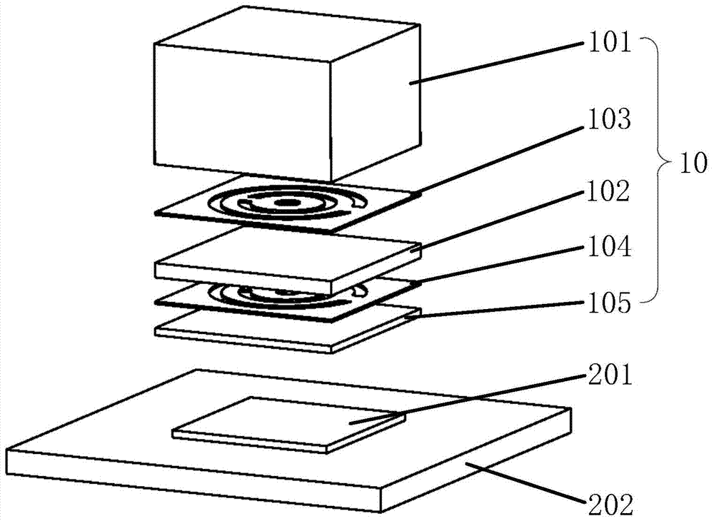
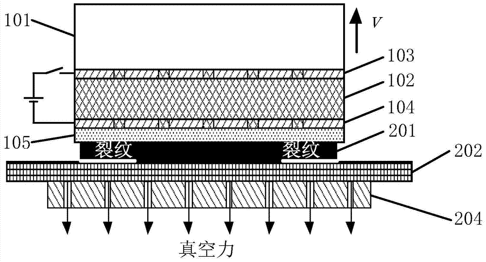
[0048] See figure 1 As shown, the main structure part 10 of the electronic device transfer device constructed according to the embodiment of the present invention includes an elastic adapter body 101 with a certain pressure buffering effect; Electrode layer 103; Undertaking the lower surface of the upper electrode layer 103 is the electroactive layer 102; The lower electrode layer 104 is attach...


PUM


Abstract

The invention discloses a device for electronic device transfer. The device comprises an upper electrode layer, a lower electrode layer, a viscous layer and an electrical active layer, wherein the upper electrode layer and the lower electrode layer are arranged oppositely in a spaced mode, an electric field can be generated between the upper electrode layer and the lower electrode layer after electrification, the viscous layer is fixedly connected to the lower surface of the lower electrode layer, the electrical active layer is arranged between the upper electrode layer and the lower electrode layer and can be squeezed to deform longitudinally or horizontally under the action of the electric field generated between the two electrode layers after electrification, the deformation of the electrical active layer drives the electrode layers and the viscous layer to deform so that shearing force and / or concave-convex ejecting force can be generated, and then the electrode layers and the viscous layer are debonded to be placed on a receptor substrate. The invention further discloses a method for electronic device transfer by means of the device and the application of the device. The method and device can be used for active placing of electronic devices. The device is simple in structure, quick and reliable in use, easy to control and the like. The method and device can be used for transfer of ordinary ultrathin and flexible electronic devices in various specifications as well as transfer of large-area array micro-electronic devices / structures.

Description

technical field [0001] The invention relates to the field of microelectronic packaging and manufacturing, in particular to a device, method and application for transferring electronic devices of different sizes and thicknesses. Background technique [0002] At present, electronic devices are developing rapidly under the huge market demand. Flexible electronic technology has opened up a broader application area, such as smart skin, electronic paper, flexible display, etc. Flexible electronics requires electronic devices such as IC chips, electronic structures, and integrated micro-devices to have a certain ability to adapt to curved surfaces, driving electronic devices to become thinner and thinner. At present, the thickness of IC chips used in experiments has reached 10 μm. However, ultra-thin devices are extremely easy to bend and break, and are not easy to withstand great impact, which brings great challenges to the current transfer technology of devices from donors to re...

Claims


Application Information

Patent Timeline
Patent Type & Authority Patents(China)
IPC IPC(8): H01L21/687H01L21/677
CPCH01L21/677H01L21/683
Inventor 黄永安徐洲龙刘尊旭高嵩刘慧敏尹周平
Owner HUAZHONG UNIV OF SCI & TECH
Why Eureka
Try Eureka