Surface conduction electron emission source structure and manufacturing method thereof

A technology for conduction electrons and electron emission, which is applied in the manufacture of thermionic cathodes, cathode ray tubes/electron beam tubes, circuits, etc. Low efficiency and other problems, to achieve the effect of low equipment requirements, improved field emission electron efficiency, and easy scattering

Active Publication Date: 2017-08-01
XI AN JIAOTONG UNIV
View PDF7 Cites 0 Cited by
  • Summary
  • Abstract
  • Description
  • Claims
  • Application Information

AI Technical Summary

Problems solved by technology

However, the basic principle of the "power-on formation" process is to use the Joule heat generated by power-on to heat and "burn" the electron emission film, its position and width are random, and the consistency between the various electron emission units is poor , which affects the performance of the electron emission source, making the current density and electron emission efficiency of the surface conduction electron emission source lower

Method used


Image

  • Surface conduction electron emission source structure and manufacturing method thereof
  • Surface conduction electron emission source structure and manufacturing method thereof
  • Surface conduction electron emission source structure and manufacturing method thereof

Examples


Embodiment 1

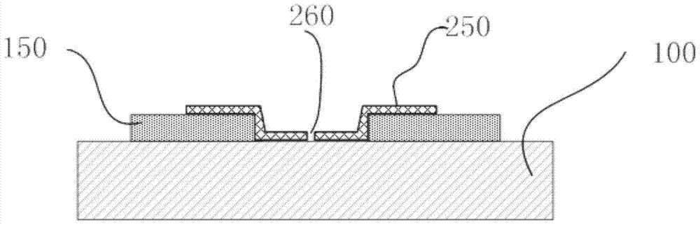
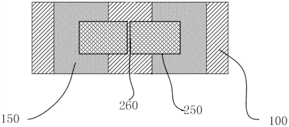
[0049] see Pic 4-1 and Figure 4-2 , a surface conduction electron emission source structure with a raised center, including two device electrodes 150, a protruding dielectric 310 and an electron emission film 250 located in the middle of the electrode gap.

[0050] The process of making this structure is:

[0051] 1) Using magnetron sputtering or other methods to sputter several groups of metal electrodes 150 on the substrate 100 to form an electrode array, the thickness of the electrodes is 100-200 nm, and there is a gap of 8-20 μm between the electrodes;

[0052] 2) Sputter a layer of protruding dielectric 310 between the device electrodes 150 with a width of 2-5 μm, a length equivalent to that of the surface conduction electron emission film 250, and a thickness of 100-150 nm between the device electrodes 150 by means of magnetron sputtering;

[0053] 3) sputtering a surface conduction electron emission film 250 between the device electrodes 150 by means of magnetron sp...

Embodiment 2

[0056] see Figure 5-1 and Figure 5-2 , a surface conduction electron emission source structure with one side raised, the structure includes two device electrodes 150, one side is connected to the electrodes, a dielectric filling layer 300 and an electron emission film 250 filling part of the gap between the electrodes.

[0057] The process of making this structure is:

[0058] 1) Using magnetron sputtering or other methods to sputter several groups of metal electrodes 150 on the substrate 100 to form an electrode array, the thickness of the electrodes is 100-200 nm, and there is a gap of 8-20 μm between the electrodes;

[0059] 2) Use magnetron sputtering or other methods to sputter a dielectric filling layer 300 with a thickness equivalent to the thickness of the electrodes between the device electrodes 150, fill the dielectric filling layer 300 with a width of 4-8 μm, one side of which is connected to one end of the electrode, and the other side in the electrode gap.

...

Embodiment 3

[0063] see Figure 6-1 and Figure 6-2 , a surface conduction electron emission source structure with a filled middle pad, including two device electrodes 150 , a dielectric filling layer 300 , a protruding dielectric 310 and an electron emission film 250 .

[0064] During fabrication, the dielectric filling layer 300 is fabricated first, and then the protruding dielectric 310 is fabricated. The specific fabrication steps are as follows:

[0065] 1) Using magnetron sputtering or other methods to sputter several groups of metal electrodes 150 on the substrate 100 to form an electrode array, the thickness of the electrodes is 100-200 nm, and there is a gap of 8-20 μm between the electrodes;

[0066] 2) Sputtering a dielectric filling layer 300 with a thickness equivalent to the electrode thickness between the device electrodes 150 to fill the electrode gap by magnetron sputtering or other methods;

[0067] 3) sputtering a layer of protruding dielectric 310 between the device e...


PUM


Abstract

The invention discloses a surface conduction electron emission source structure and a manufacturing method of the surface conduction electron emission source structure, and belongs to the technical field of flat panel display manufacturing. The surface conduction electron emission source structure comprises a pair of symmetric device electrodes deposited on a substrate. An electron emission thin film is deposited on the device electrodes, and a nanometer crack is formed in the electron emission thin film. An 8-micrometer-to-20-micrometer electrode gap is formed between the symmetric device electrodes, and a dielectric filling layer and / or protruding dielectric are / is arranged in the electrode gap. The manufacturing method includes the steps that a protrusion is firstly built in the middle of the electrode gap; then a conductive film is manufactured on the protrusion; according to the characteristic that materials of the protrusion are poor in heat conductivity and the difference between the portion, covering the protrusion, of the conductive film and the other portions of the conductive film in geometric position, more joule heat is generated at the portion, covering the protrusion, of the conductive film during power-on forming, and the nanometer crack can be formed at the protrusion. Controllable manufacturing of the nanometer crack in position can be achieved, and the electron field emission efficiency can be improved.

Description

technical field [0001] The invention belongs to the technical field of flat panel display manufacturing, and relates to a surface conduction electron emission source structure and a manufacturing method thereof, in particular to a surface conduction electron emission source structure capable of controlling the formation position of nano cracks in a surface conduction electron emission film and a manufacturing method thereof. Background technique [0002] The Surface-conduction Electron-emitter Display (SED) proposed by Canon Corporation of Japan is a kind of FED, and its display effect is very prominent among current flat panel display devices. [0003] The imaging principle of SED is similar to the traditional cathode ray tube (Cathode Ray Tube, CRT). Unlike CRT, SED puts the glass plate coated with fluorescent material in parallel with the glass bottom plate covered with a large number of surface conduction electron emission sources. , such a structure makes the thickness ...

Claims


Application Information

Patent Timeline
Patent Type & Authority Patents(China)
IPC IPC(8): H01J29/04H01J9/04
CPCH01J9/04H01J29/04
Inventor 吴胜利王晓张劲涛沈志华胡文波
Owner XI AN JIAOTONG UNIV
Why Eureka
Try Eureka