Array substrate of organic electroluminescence display panel, manufacturing method and display device

An electroluminescence display and array substrate technology, which is applied to circuits, electrical components, electrical solid devices, etc., can solve the problems of polyimide material residue, complex manufacturing processes of pixel defining layers and spacers, etc., and achieves enhanced adhesion. The effect of adhesion, reducing one-time curing treatment, and simplifying the production process

Active Publication Date: 2018-03-23
BOE TECH GRP CO LTD
View PDF4 Cites 0 Cited by
  • Summary
  • Abstract
  • Description
  • Claims
  • Application Information

AI Technical Summary

Problems solved by technology

It can be seen from this that the manufacturing process of the pixel defining layer and the spacer is relatively complicated.
[0004] In order to simplify the manufacturing process of the pixel defining layer and the spacer, the pattern of the pixel defining layer and the spacer can be formed by a patterning process using a gray tone mask first, and then the pattern of the pixel defining layer and the spacer is cured, However, the graphics of the pixel definition layer and the spacer produced by this manufacturing process will have the problem of polyimide material residue

Method used


Image

  • Array substrate of organic electroluminescence display panel, manufacturing method and display device
  • Array substrate of organic electroluminescence display panel, manufacturing method and display device
  • Array substrate of organic electroluminescence display panel, manufacturing method and display device

Examples


Embodiment Construction

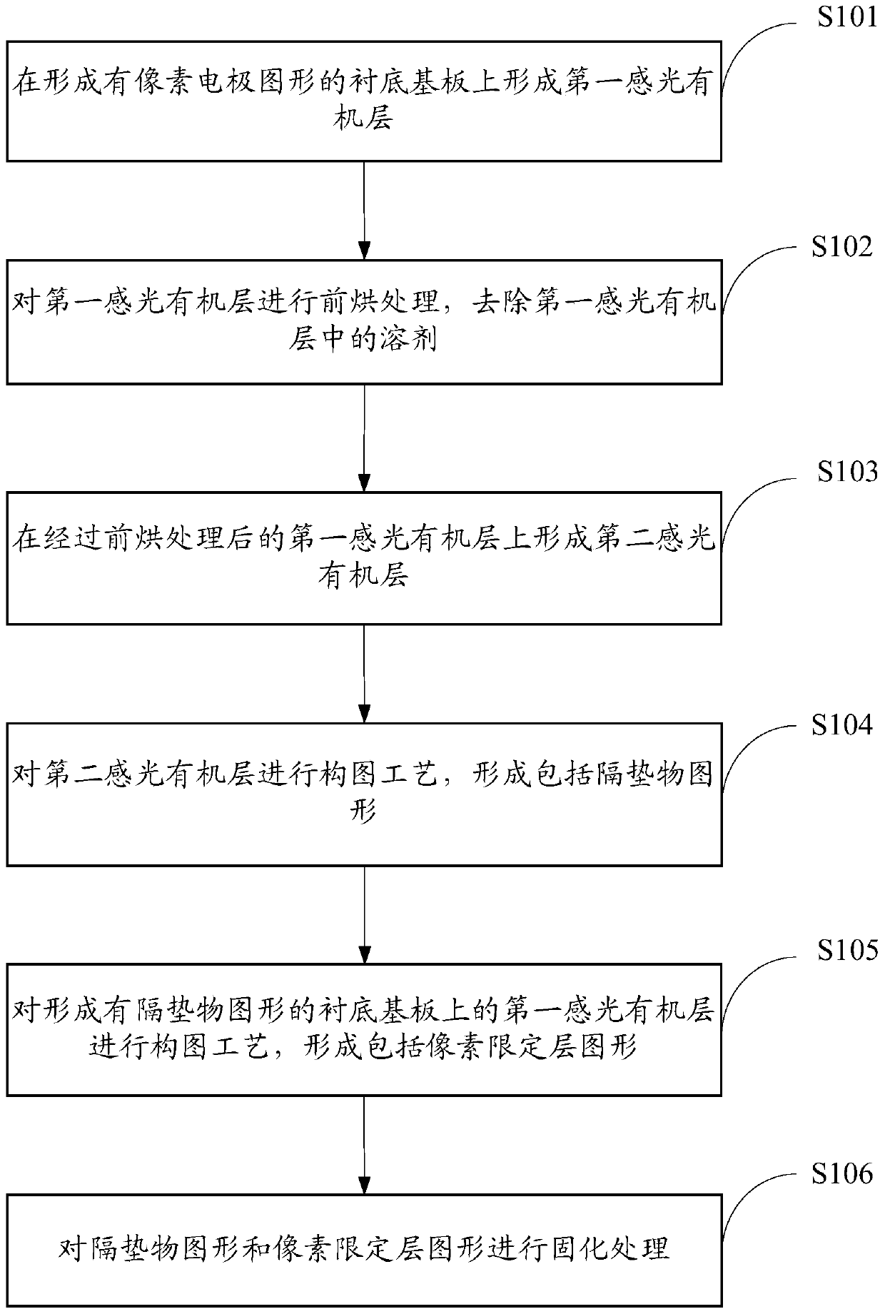
[0034] The specific implementations of the array substrate, manufacturing method and display device of the organic electroluminescence display panel provided by the embodiments of the present invention will be described in detail below with reference to the accompanying drawings.

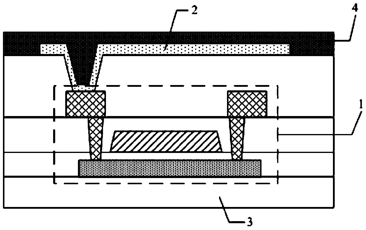
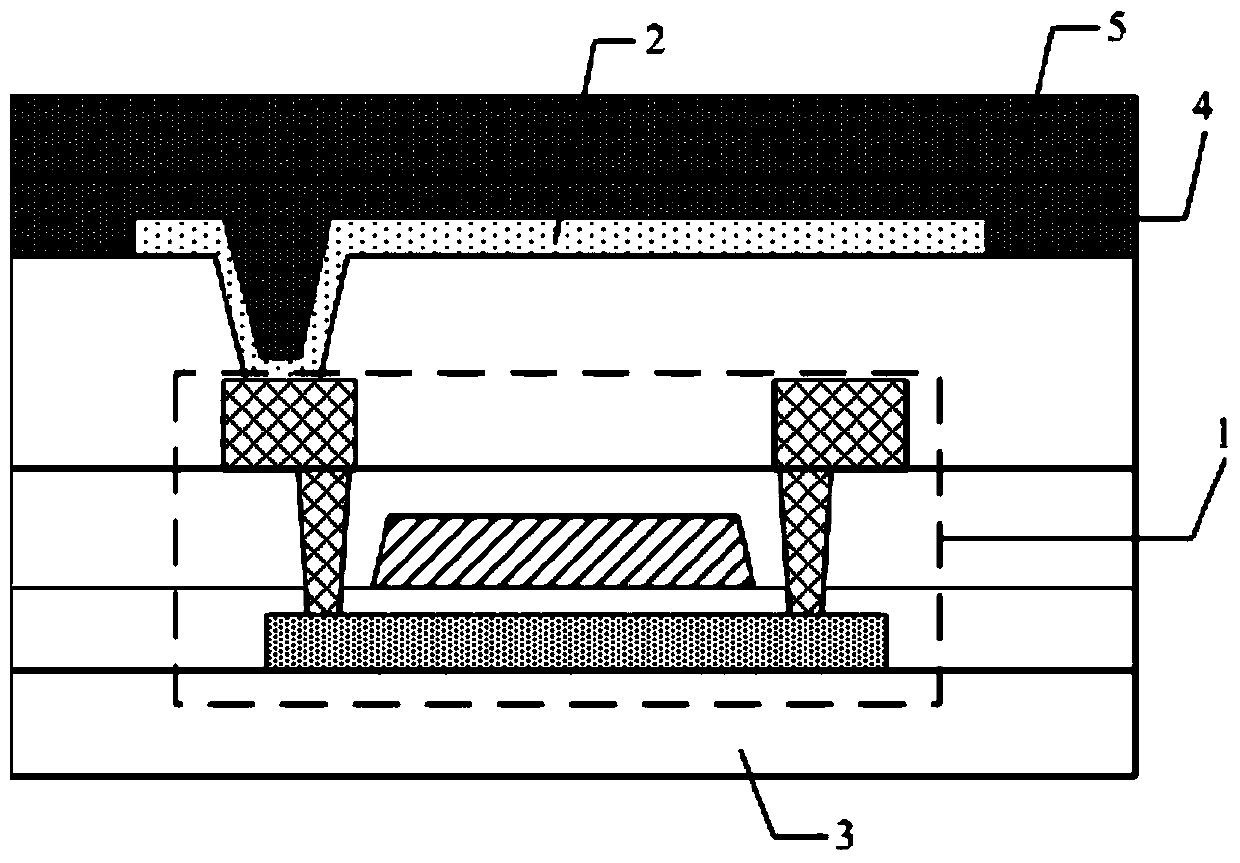
[0035] The shape and thickness of each film layer in the drawings do not reflect the real proportion of the array substrate, but are only intended to schematically illustrate the content of the present invention.

[0036] A method for fabricating an array substrate of an organic electroluminescent display panel provided by an embodiment of the present invention, such as figure 1 shown, including the following steps:

[0037] S101, forming a first photosensitive organic layer on the base substrate on which the pixel electrode pattern is formed;

[0038] S102. Pre-baking the first photosensitive organic layer to remove the solvent in the first photosensitive organic layer;

[0039] S103, forming a s...


PUM


Abstract

The invention discloses an array substrate of an organic electroluminescence display panel, a manufacturing method and a display device. In the manufacturing method of the array substrate, after the first photosensitive organic layer is formed, the first photosensitive organic layer is pre-baked , remove the solvent in the first photosensitive organic layer, to enhance the adhesion between the first photosensitive organic layer and the film layer where the pixel electrode is located, and reduce the photosensitivity of the first photosensitive organic layer; after that, in the first photosensitive organic layer Form a second photosensitive organic layer on top, and perform a patterning process on the second photosensitive organic layer to form a spacer pattern, which will not affect the first photosensitive organic layer; after that, perform a patterning process on the first photosensitive organic layer to form a pixel definition layer Graphics, and one curing treatment for spacer graphics and pixel definition layer graphics; in this way, one curing treatment can be reduced, thereby simplifying the manufacturing process of spacer and pixel definition layers, and there will be no problem of organic material residue .

Description

technical field [0001] The invention relates to the field of display technology, in particular to an array substrate of an organic electroluminescence display panel, a manufacturing method and a display device. Background technique [0002] Among the existing display panels, the organic electroluminescent display panel (Organic Electroluminescent Display, OLED) has gradually become the mainstream in the display field due to its low power consumption, high color saturation, wide viewing angle and other characteristics. [0003] In the manufacturing process of the array substrate in the existing organic electroluminescent display panel, after forming the pixel electrodes, polyimide material is generally used to sequentially form the pixel definition layer for defining each pixel area of ​​the organic electroluminescent display panel And spacers for buffering external force to protect each film layer in the organic electroluminescence display panel. Specifically, the manufactu...

Claims


Application Information

Patent Timeline
Patent Type & Authority Patents(China)
IPC IPC(8): H01L21/77H01L27/32
CPCH01L27/1214H01L27/1259H01L21/77H01L2021/775H10K59/00
Inventor 许晓伟石磊龙春平
Owner BOE TECH GRP CO LTD
Why Eureka
Try Eureka