Method of fabricating image sensor

Active Publication Date: 2009-05-21
SAMSUNG ELECTRONICS CO LTD
View PDF12 Cites 15 Cited by
  • Summary
  • Abstract
  • Description
  • Claims
  • Application Information

AI Technical Summary

Benefits of technology

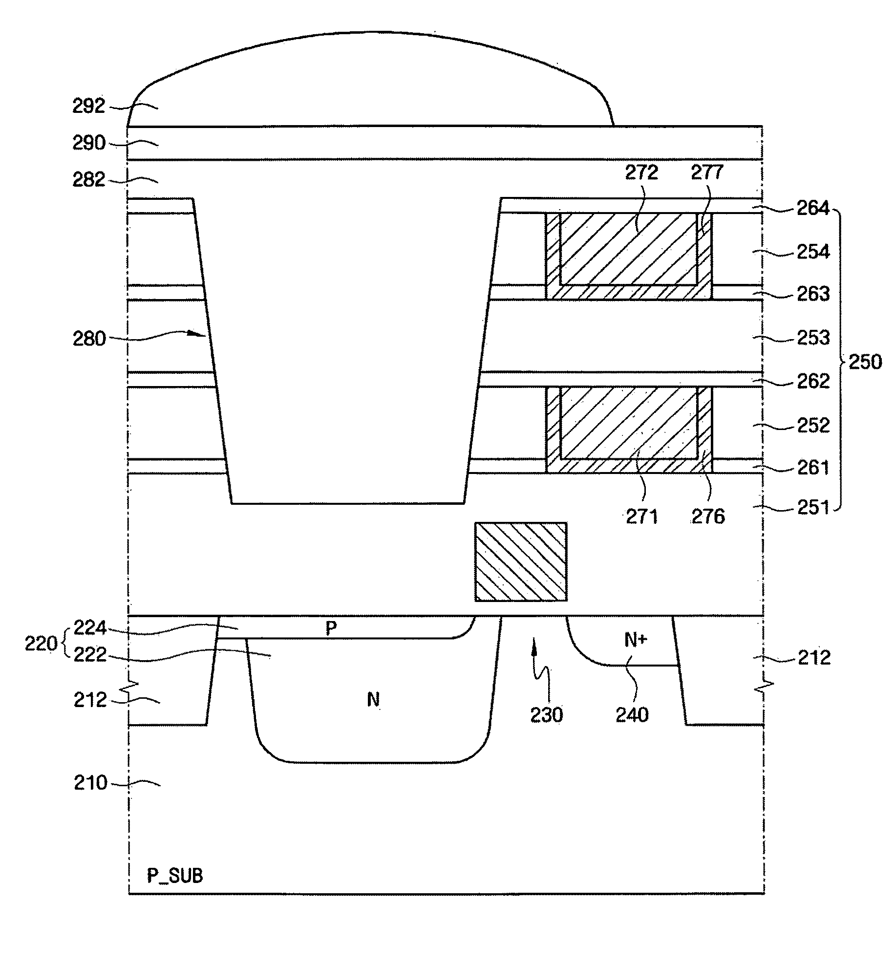
[0008]Also, on the photoelectric transformation device of a MOS image sensor, multi-layer interlayer dielectric layers to insulate multi-layer of metal interconnections, etch stop layer used for forming copper interconnections, and diffusion barrier layers to prevent diffusion of copper interconnections are formed. Here, among the layers formed on the photoelectric transformation device there can be layers that have a low light penetration ratio. For example, a silicon nitride layer used for an etch stop layer and/or diffusion barrier layer has a low light penetration ratio. In this case, the photosensitivity of an image sensor can be

Problems solved by technology

The cavity can be formed using a plasma etch process, and such a process can cause damage

Method used


Image

  • Method of fabricating image sensor
  • Method of fabricating image sensor
  • Method of fabricating image sensor

Examples


Example

EXPERIMENT EXAMPLES

[0090]The reference experiment example involved the measurement of the dark level of output signals without heat treatment or UV treatment after forming the cavity.

Example

[0091]Experiment example 1 involved the measurement of the dark level of output signals with heat treatment after forming the cavity.

Example

[0092]Experiment example 2 involved the measurement of the dark level of output signals with UV treatment after forming the cavity.


PUM


Abstract

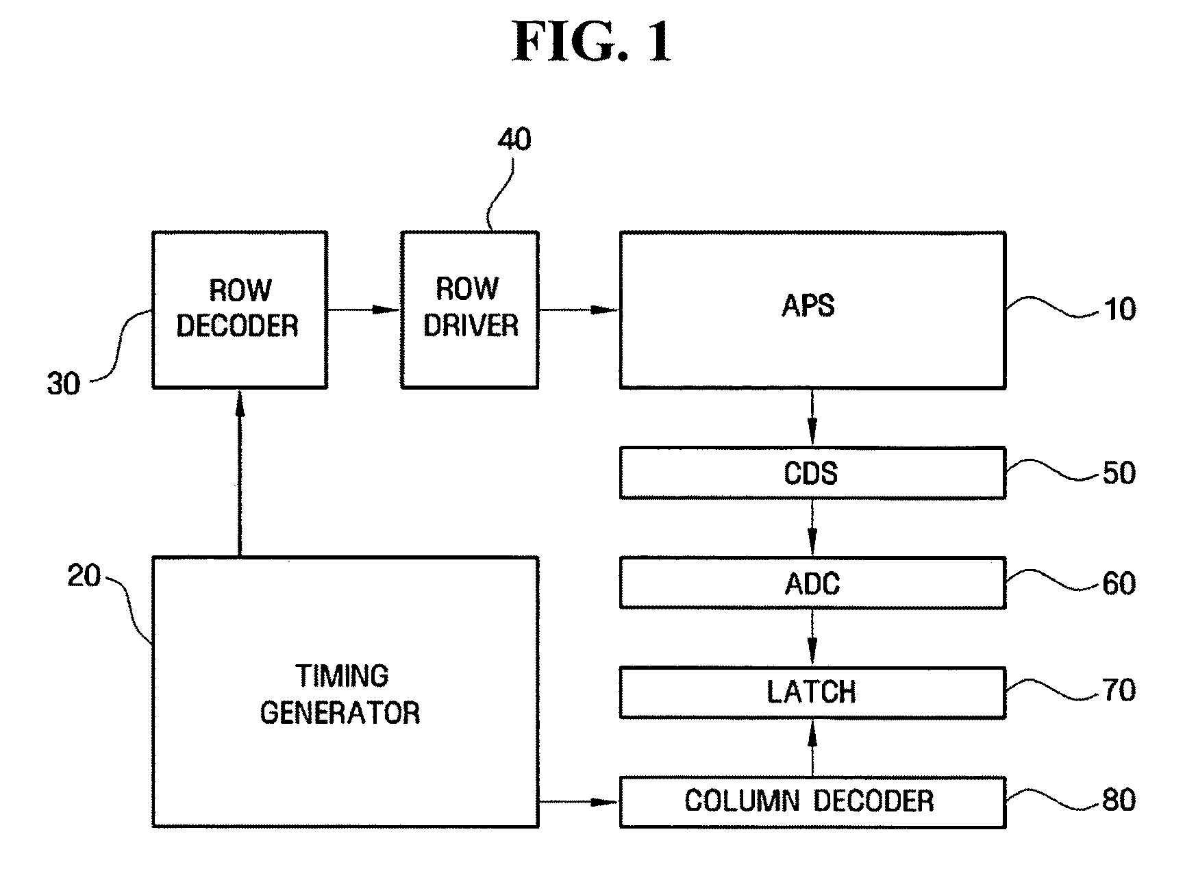
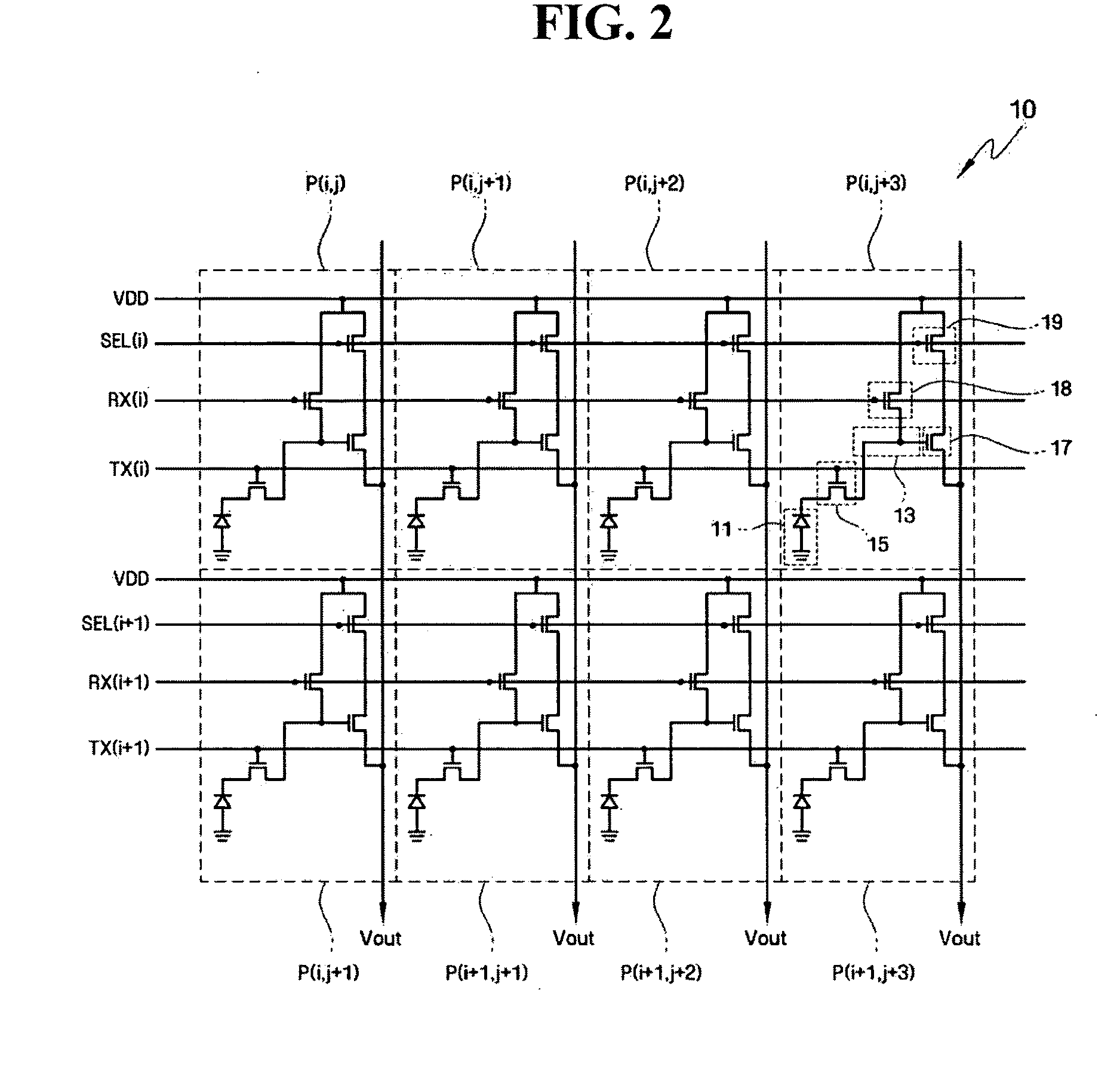
A method of fabricating an image sensor includes forming a photoelectric transformation device on a substrate and forming a dielectric layer structure on the substrate. The dielectric layer structure includes multi-layer interlayer dielectric layers and multi-layer metal interconnections which are located between the multi-layer interlayer dielectric layers. A cavity which penetrates the multi-layer interlayer dielectric layers on the photoelectric transformation device is formed. A heat treatment is performed on the substrate on which the cavity is formed.

Description

CROSS REFERENCE TO RELATED APPLICATION[0001]This application claims priority from Korean Patent Application No. 10-2007-0118136 filed on Nov. 19, 2007, in the Korean Intellectual Property Office, the contents of which are incorporated herein by reference in their entirety.BACKGROUND OF THE INVENTION[0002]1. Field of the Invention[0003]The present invention relates to a method of fabricating an image sensor.[0004]2. Description of the Related Art[0005]An image sensor transforms optical images into electrical signals. Recent advances in computer and communication industries have led to strong demands for high performance image sensors in various consumer electronic devices including digital cameras, camcorders, PCS (Personal Communication System), game devices, security cameras medical microcameras, and the like.[0006]Specially, a MOS image sensor can be readily driven and implemented using various scanning methods. Also, the size of a product can be minimized since digital signal pro...

Claims


Application Information

Patent Timeline
IPC IPC(8): H01L31/18
CPCH01L27/14687H01L27/14643H01L27/146
Inventor LEE, JEONG-HOJUNG, SANG-LLPARK, YOUNG-HOONYANG, JUN-SEOKSHIN, AN-CHULJUNG, MIN-YOUNG
Owner SAMSUNG ELECTRONICS CO LTD
Why Eureka
Try Eureka