Bumping process

a technology of bumping process and bumping plate, which is applied in the direction of semiconductor devices, semiconductor/solid-state device details, electrical apparatus, etc., can solve the problems of poor reliability of packages, short height the thickness of photoresist layer in the volume and height of bumps fabricated by the conventional bumping process, etc., to achieve reliable electrical and mechanical connection between chips and carriers, the effect of increasing the heigh

a technology of bumping process and bumping plate, which is applied in the direction of semiconductor devices, semiconductor/solid-state device details, electrical apparatus, etc., can solve the problems of poor reliability of packages, short height the thickness of photoresist layer in the volume and height of bumps fabricated by the conventional bumping process, etc., to achieve reliable electrical and mechanical connection between chips and carriers, the effect of increasing the heigh

US6930031B2Active Publication Date: 2005-08-16ADVANCED SEMICON ENG INC

Image

  • Bumping process
  • Bumping process
  • Bumping process

Examples


first embodiment

The First Embodiment

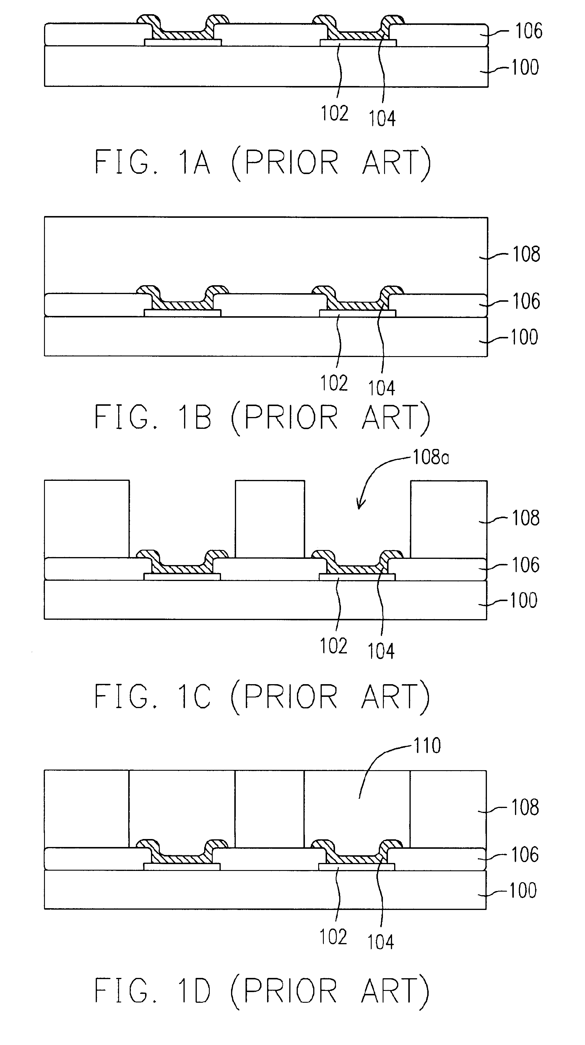
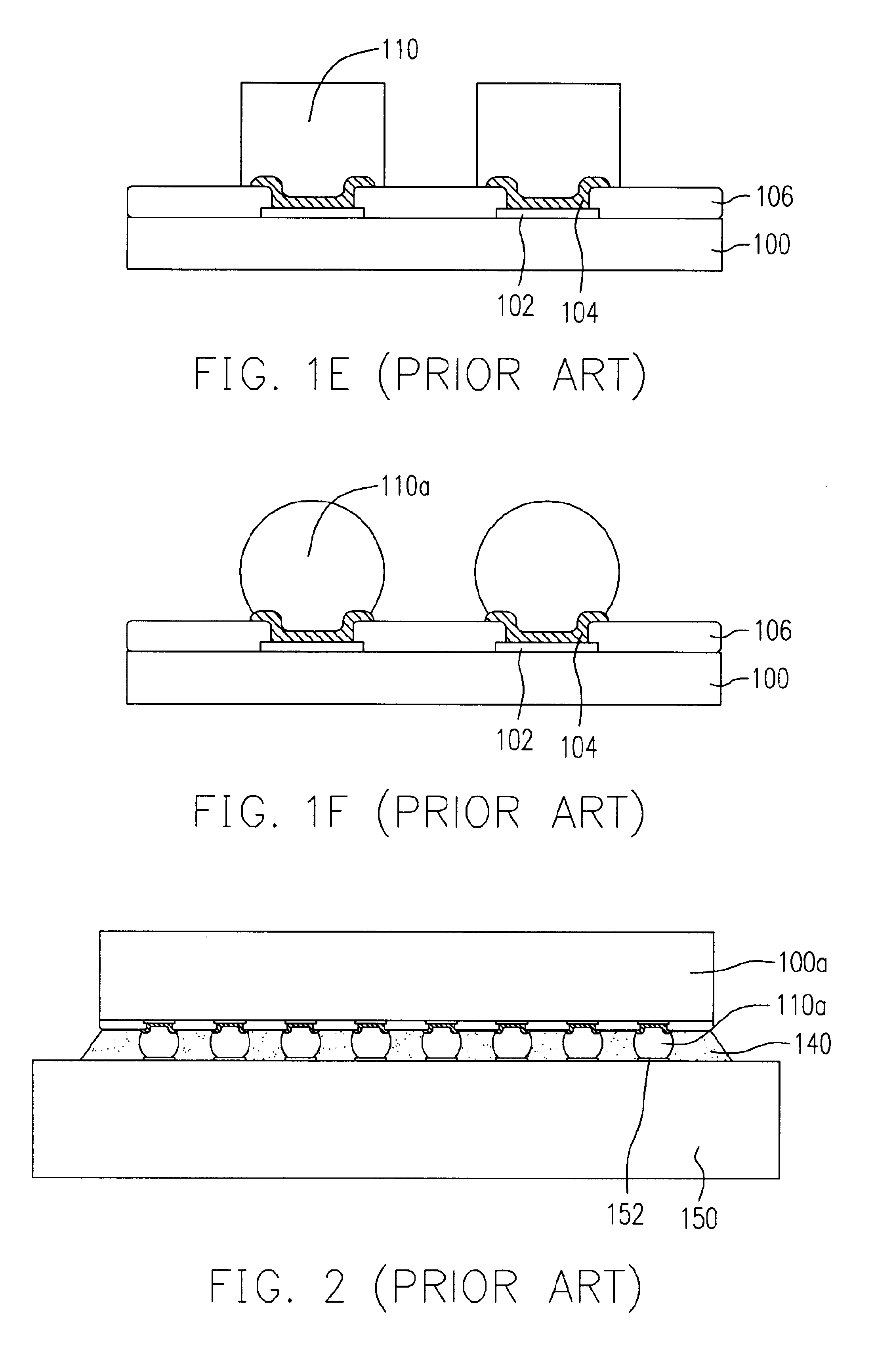
[0030]FIGS. 4A to 4F are schematic cross-sectional views of a bumping process in accordance with the first embodiment of the present invention. First, referring to FIG. 4A, a wafer 310 having, for example, a plurality of bonding pads 314 and a passivation layer 316 thereon for the protection of the wafer 310. The bonding pads 314 are exposed by the passivation layer 316. In addition, each bonding pad 314, for instance, is provided with an under bump metallurgy (UBM) layer 318 formed thereon. The process of forming the UBM layer 318 comprises forming at least a metal layer by sputtering or evaporation, for example, and then patterning the metal layer. The under bump metallurgy layer 318, for example, consists of three layers, i.e., an adhesion layer / a barrier layer / a wetting layer. The adhesion layer enhances bonding between the UBM layer 318 and the bonding pad 314. The barrier layer can act to prevent mobile ions from penetrating the UBM layer 318 and dispersing...

second embodiment

The Second Embodiment

[0035]The second embodiment of the present invention discloses a method to obtain bumps with the higher height. FIGS. 5A to 5F are schematic cross-sectional views of a bumping process in accordance with the second embodiment of the present invention. Referring first to FIG. 5A, a wafer 410 is provided with a plurality of bonding pads 414, and a passivation layer 416 thereon for the protection of the wafer 410. The bonding pads 414 are exposed by the passivation layer 416. For each bonding pad 414, an under-bump-metallurgy (UBM) layer 418 is formed on the bonding pad 414.

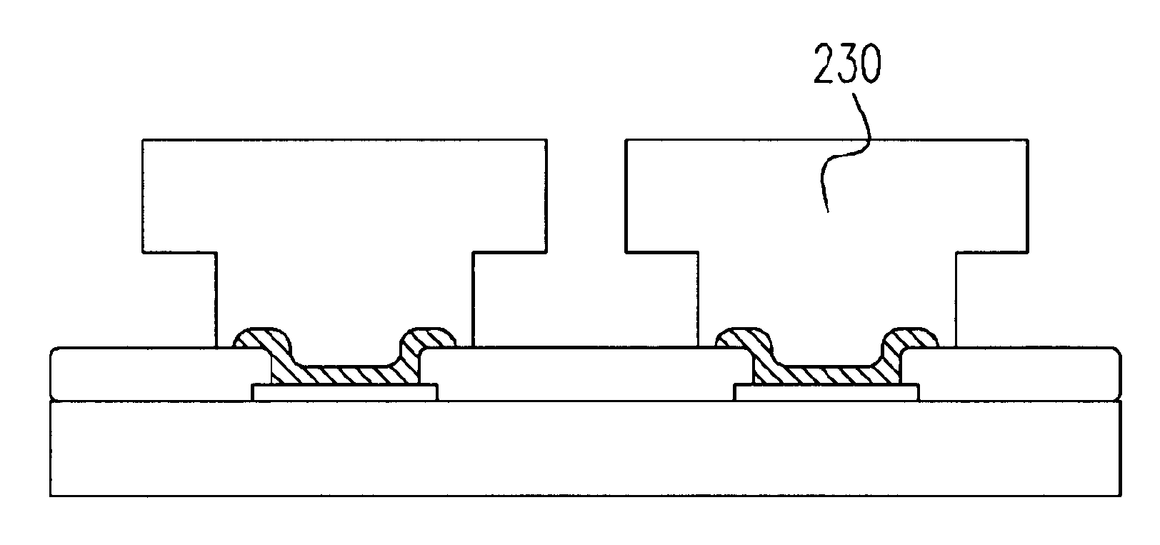
[0036]Referring to FIG. 5B, a plurality of photoresist layers 420 is formed over the wafer 410 and covers the UBM layer 418 and the passivation layer 416. Among the photoresist layers 420, the topmost photoresist layer 420 (i.e., farthest away from the bonding pad 414), for instance, has the highest photosensitivity and the fastest development rate, while the bottommost photoresist layer (i.e., c...


PUM


Abstract

A bumping process is disclosed. The bumping process comprises the steps of: providing a wafer having a plurality of bonding pads and a passivation layer, wherein the passivation layer exposes the bonding pads; forming an UBM layer over the wafer to cover the bonding pads; forming two or more photoresist layers over the wafer, wherein the photoresist layers have different exposure and development characteristics; forming at least one or more stair-shaped openings in the photoresist layers by a single exposure corresponding to the bonding pads; filling solder into the stair-shaped openings to form a plurality of solder bumps; removing the entire photoresist layer. The bumping process can provide bumps with higher heights, so that the connection between chips and carriers becomes more reliable.

Description

CROSS REFERENCE TO RELATED APPLICATIONS[0001]This application claims the priority benefit of Taiwan application serial no. 92120367, filed Jul. 25, 2003.BACKGROUND OF INVENTION[0002]1. Field of the Invention[0003]The present invention relates to bumping process, and in particular, to a bumping process to fabricate bumps with the higher height which enhances connection reliability between chips and a carrier by way of a single exposure to form stair-shaped openings in the photoresist layer.[0004]2. Description of the Related Art[0005]In the modern world with abundant information, the market of multi-media application is thus continuously growing. The development of Integrated Circuits (IC) packaging technology should be in line with the development of electronic devices, including digitization, network development, local area connections and user friendliness of electronic devices. To meet the above requirements, capacities of high-speed processing, multi-function, miniaturization, l...

Claims


Application Information

Patent Timeline
16 Aug 2005
Publication
US6930031B2
IPC
H01L21/02; H01L21/60; H01L23/485; H01L23/48
CPC
H01L24/11; H01L24/13; H01L2924/0001; H01L2224/11474; H01L2224/13099; H01L2924/01013; H01L2924/01022; H01L2924/01029
Inventors
HUANG, MIN-LUNG