Semiconductor device, metal-insulator-metal capacitor and method for manufacturing same

A technology of metal capacitors and manufacturing methods, which is applied in semiconductor/solid-state device manufacturing, semiconductor devices, semiconductor/solid-state device components, etc., can solve the problems of pixel photosensitive loss, large space occupation, and high metal layer thickness, so as to reduce lateral Effect of optical crosstalk and space reduction

Active Publication Date: 2009-09-16
BRIGATES MICROELECTRONICS KUNSHAN
View PDF1 Cites 14 Cited by
  • Summary
  • Abstract
  • Description
  • Claims
  • Application Information

AI Technical Summary

Problems solved by technology

[0012] The technical problem to be solved by the present invention is that the MIM capacitor manufactured by the existing CMOS process takes up a large space in the CMOS image sensor, and the thickness of the metal layer is too high, which will cause photosensitive loss to the pixels at the edge of the pixel array.

Method used


Image

  • Semiconductor device, metal-insulator-metal capacitor and method for manufacturing same
  • Semiconductor device, metal-insulator-metal capacitor and method for manufacturing same
  • Semiconductor device, metal-insulator-metal capacitor and method for manufacturing same

Examples


Embodiment Construction

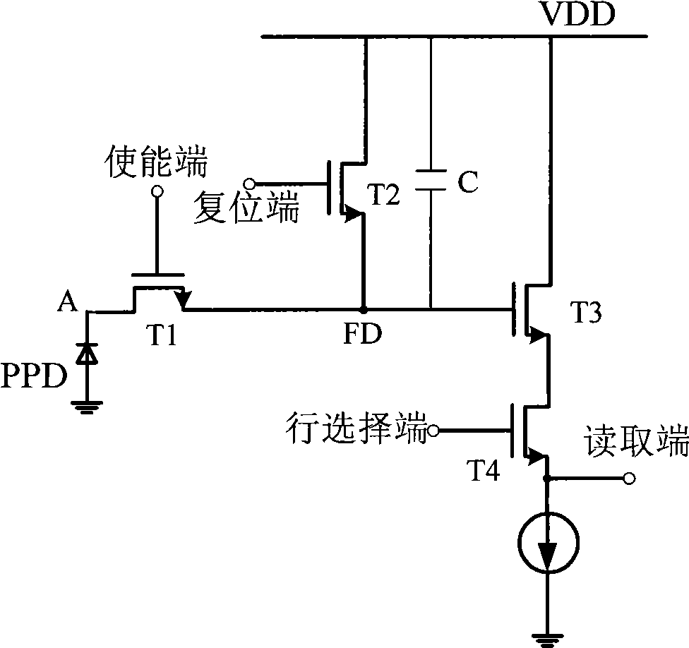
[0041] An embodiment of the metal-insulator-metal capacitor manufacturing method provided by the present invention is as follows: Figure 5 As shown, it mainly includes the following steps:

[0042] 11) providing a semiconductor substrate, depositing a first metal layer on the semiconductor substrate;

[0043] 12) patterning the first metal layer;

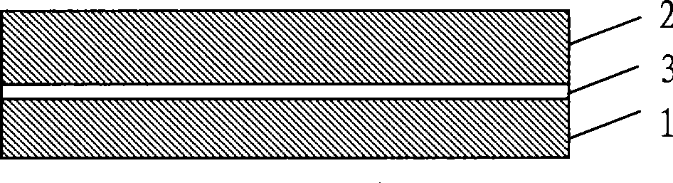
[0044] 13) depositing a passivation layer on the first metal layer;

[0045] 14) etching the passivation layer to form wiring holes;

[0046] 15) depositing a dielectric layer on the surface of the passivation layer;

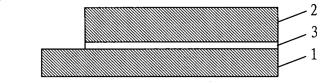
[0047] 16) Etching part of the dielectric layer, retaining the required dielectric layer for making MIM capacitors;

[0048] 17) Covering and depositing a second metal layer on the surface of the dielectric layer and the passivation layer.

[0049] In the above embodiment, the passivation layer and the wiring hole are first formed on the first metal layer, and the required dielectric layer is formed according to...


PUM


Abstract

The invention provides a semiconductor device, a metal-insulator-metal (MIM) capacitor and a method for manufacturing the same, wherein the method comprises the following steps: depositing a first metal layer on a semiconductor substrate and patterning the metal layer; depositing a passivation layer on the first metal layer and forming a connecting line hole thereon by etching; depositing a dielectric layer on the surfaces of the passivation layer and the connecting line hole and etching part of the dielectric layer; covering and depositing a second metal layer on the surfaces of the dielectric layer and the passivation layer; and using the first metal layer as a lower electrode plate and the second metal layer as an upper electrode plate. The MIM capacitor combines the upper electrode plate metal layer with a metal interconnection layer, reduces the space occupied in the semiconductor device, avoids influencing the photosensitive property of edge pixels in a pixel array, and can achieve the aim of reducing lateral light crosstalk by arranging the position and the number of the connecting line hole reasonably.

Description

technical field [0001] The present application relates to the field of CMOS process manufacturing, and in particular to a semiconductor device, a metal-insulator-metal (Metal-Insulator-Metal, MIM) capacitor and a manufacturing method thereof. Background technique [0002] A CMOS image sensor (CIS), which is a semiconductor device that converts an optical image from an optical signal to an electrical signal, employs a switching mode to sequentially detect pixel outputs by providing a predetermined number of MOS transistors to each pixel. The key to determining the image quality of a CMOS image sensor is dark current and dynamic range. [0003] like figure 1 A pixel unit circuit of a four-tube structure CMOS image sensor is shown. It mainly includes a photodetector PDD, a transmission tube T1, a reset tube T2, a source follower T3, and a selection tube T4. The photodetector PDD includes a photodiode that generates charges from light energy and integrates the charges at poin...

Claims


Application Information

Patent Timeline
Patent Type & Authority Applications(China)
IPC IPC(8): H01L21/02H01L21/768H01L27/04H01L27/146H01L23/522H01L29/92
Inventor 周谨
Owner BRIGATES MICROELECTRONICS KUNSHAN
Why Eureka
Try Eureka