Semiconductor device and manufacturing method thereof

A semiconductor and nitride semiconductor technology, applied in semiconductor/solid-state device manufacturing, semiconductor devices, electrical components, etc., can solve problems such as increasing current leakage and doping conditions

Active Publication Date: 2020-01-14
SEOUL VIOSYS CO LTD
View PDF8 Cites 0 Cited by
  • Summary
  • Abstract
  • Description
  • Claims
  • Application Information

AI Technical Summary

Problems solved by technology

However, current leakage may increase depending on doping conditions due to insufficient growth process of the p-type semiconductor layer for filling the V-pit

Method used


Image

  • Semiconductor device and manufacturing method thereof
  • Semiconductor device and manufacturing method thereof
  • Semiconductor device and manufacturing method thereof

Examples


no. 1 example

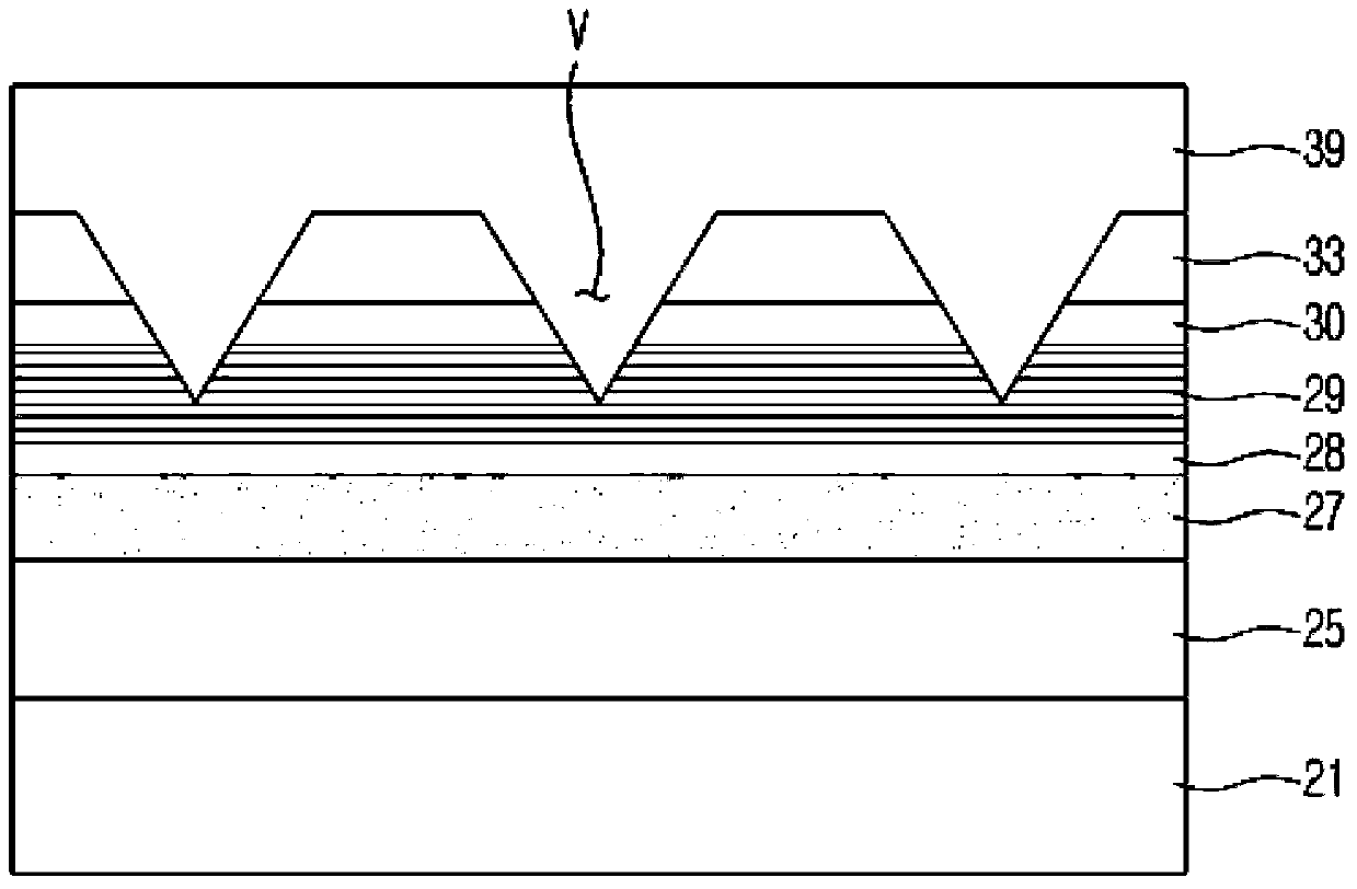
[0057] According to the first embodiment of the present invention, the nitride semiconductor layer has V-pit V with larger size and higher density, so as to effectively prevent damage to the device due to electrostatic discharge. Specifically, the structure and configuration of the nitride semiconductor device can be applied to various types of semiconductor devices including light emitting diodes, laser diodes, transistors, and the like.

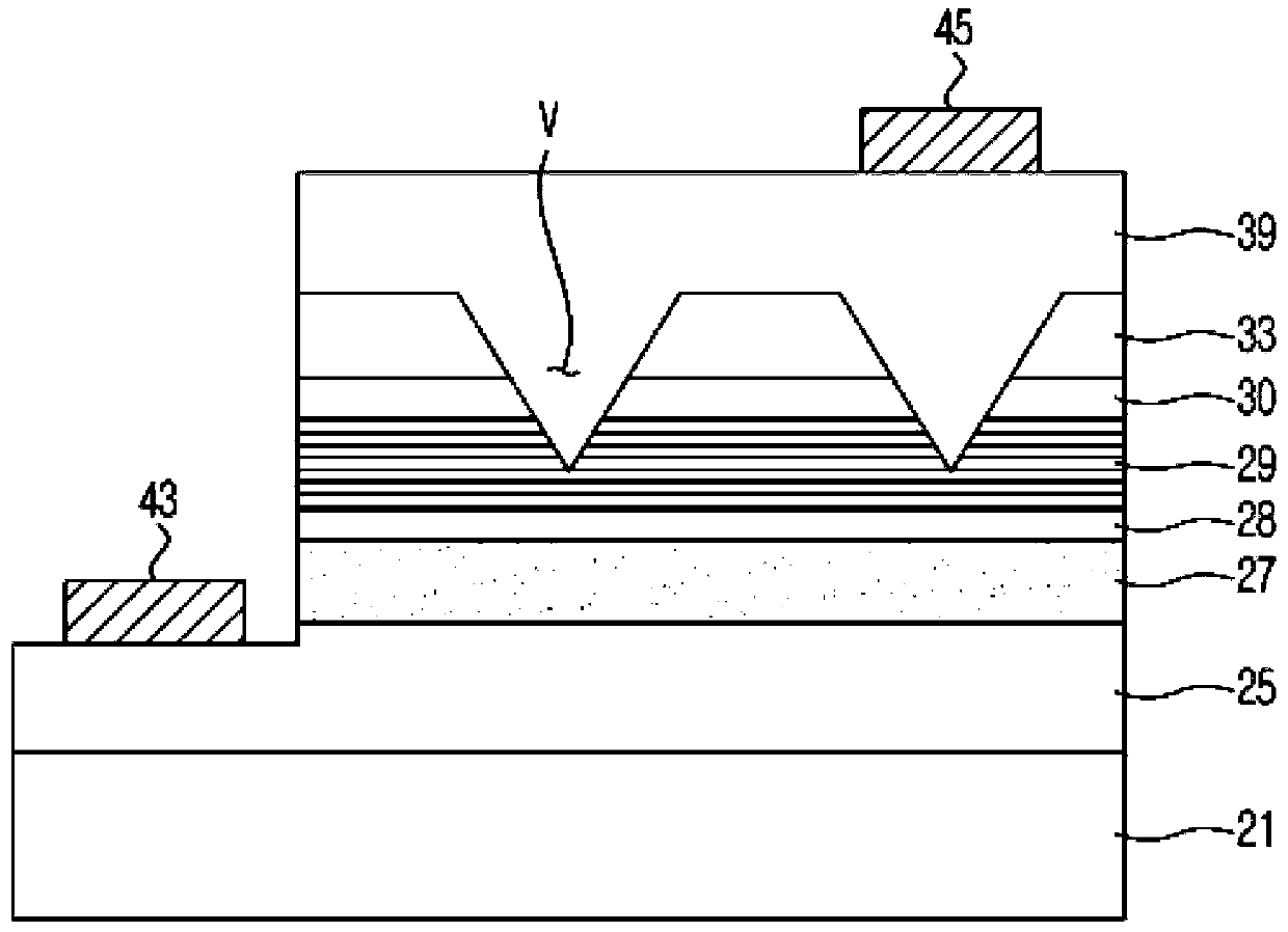
[0058] figure 2 is a cross-sectional view of a semiconductor device according to a second embodiment of the present invention. figure 2 An example of a light emitting diode using the nitride semiconductor device according to the first embodiment is shown, but it should be understood that the present invention is not limited thereto.

[0059] refer to figure 2 , the nitride semiconductor device (ie, light emitting diode) according to the second embodiment of the present invention may include a first conductivity type semiconductor layer...


PUM

PropertyMeasurementUnit
thicknessaaaaaaaaaa
thicknessaaaaaaaaaa
thicknessaaaaaaaaaa

Abstract

Disclosed a semiconductor device and a method of manufacturing thereof. The semiconductor apparatus comprises: a first conductive semiconductor layer, comprising a first conductive semiconductor layer and an upper conductive semiconductor layer; V-pit, passing through at least part of the first upper conductive semiconductor layer; The second conductive semiconductor layer, located on the first conductive semiconductor layer and filled with V-pits; And the active layer, inserted between the first conductive semiconductor layer and the second conductive semiconductor layer, V- pit through the active layer, wherein the first upper conductive semiconductor layer having a higher defect density than the first conductive semiconductor layer, and the first upper conductive semiconductor layer comprises a V- pit generating layer comprising the starting point of the V- pit. Semiconductor devices include V-pits with large size and high density, thereby effectively preventing damage to semiconductor devices due to electrostatic discharge.

Description

[0001] This application claims Korean Patent Application No. 10-2013-0128589 filed on October 28, 2013, Korean Patent Application No. 10-2014-0045933 filed on April 17, 2014, filed on August 14, 2014 Korean Patent Application No. 10-2014-0106024 filed, Korean Patent Application No. 10-2014-0106025 filed on August 14, 2014, and Korean Patent Application No. 10-2014-0106026 filed on August 14, 2014 Priority and benefit of patent applications, as fully set forth herein, are hereby incorporated by reference for all purposes. technical field [0002] The present invention relates to a semiconductor device and a method of manufacturing the semiconductor device, and more particularly, to a semiconductor device capable of improving electrostatic discharge characteristics and a method of manufacturing the semiconductor device. Background technique [0003] Nitride semiconductors are used as light sources for display devices, signal lamps, lighting devices, and optical communication d...

Claims


Application Information

Patent Timeline
Patent Type & Authority Patents(China)
IPC IPC(8): H01L29/06H01L29/36H01L21/18
CPCH01L29/155H01L29/2003H01L29/201H01L29/205H01L29/0607H01L21/02458H01L21/02513H01L21/0254H01L21/02576H01L21/0262H01L33/20H01L33/04H01L33/025H01L33/22H01L33/02
Inventor 郭雨澈崔承奎金材宪郑廷桓白龙贤张三硕洪竖延郑渼暻
Owner SEOUL VIOSYS CO LTD
Why Eureka
Try Eureka