Method for testing high-frequency chip wafers through multi-channel probe card

A technology of wafer testing and probe card, which is applied in the field of testing high-frequency chip wafers using multi-channel probe cards, can solve the problems of long test time and high test success rate, reduce crosstalk, shorten transmission time, save cost effect

Active Publication Date: 2015-05-13
SHANDONG HUAYI MICRO ELECTRONICS
View PDF5 Cites 5 Cited by
  • Summary
  • Abstract
  • Description
  • Claims
  • Application Information

AI Technical Summary

Problems solved by technology

In this case, the probability of crosstalk is minimized, and the test success rate is high, but the test time is long and unacceptable

Method used


Image

  • Method for testing high-frequency chip wafers through multi-channel probe card
  • Method for testing high-frequency chip wafers through multi-channel probe card

Examples


Embodiment Construction

[0027] In order to facilitate those skilled in the art to better understand the present invention, the present invention will be described in further detail below in conjunction with the accompanying drawings and specific embodiments. The following is only exemplary and does not limit the protection scope of the present invention.

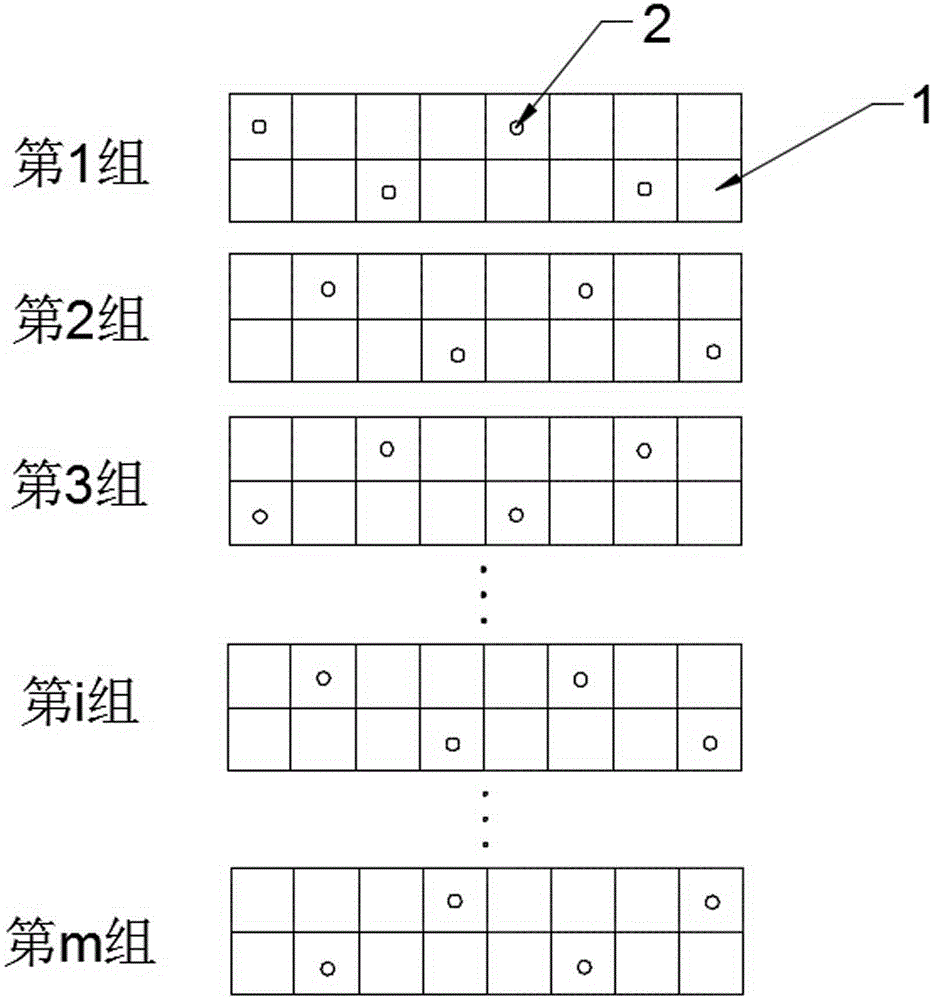
[0028] A method for testing high-frequency chip wafers using a multi-channel probe card, such as figure 1 As shown, the channels of the probe card are arranged symmetrically in two rows, that is, the number of channels and the arrangement of the two rows are the same as an example, including the following steps:

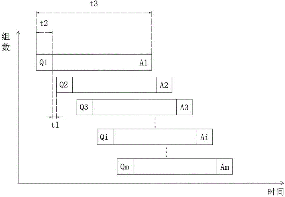
[0029] (1) Group the probe card channels, divide the probe card channels into 4 groups, each group of probe card channels includes 4 working channels, each working channel transmits an instruction, and the adjacent working channels in each group of probe card channels The channels are arranged in adjacent rows and columns, and the adjace...


PUM


Abstract

The invention discloses a method for testing high-frequency chip wafers through a multi-channel probe card. The method comprises reasonably grouping probe card channels to distribute a working channel and then transmitting instructions in a time-divided mode. Compared with parallel transmission of all the channels, by reasonably grouping the channels without adjusting intervals of the probe card channels, the method for testing the high-frequency chip wafers through the multi-channel probe card can achieve channel interval increasing and greatly reduce crosstalk, and meanwhile save redesign of the probe card and greatly reduce the cost. Compared with serial transmission, by transmitting the instructions in the time-divided mode, the method for testing the high-frequency chip wafers through the multi-channel probe card can make full use of quiet periods at instruction transmission intervals to transmit the instructions, thereby greatly shortening the transmission time; what's more, the last group of transmitted instructions and the first group of returned instructions can avoid overlapping, and the bit error rate can be reduced.

Description

technical field [0001] The invention relates to a method for testing a wafer, in particular to a method for testing a high-frequency chip wafer by using a multi-channel probe card. Background technique [0002] The high-frequency chip manufacturing process is mainly divided into IC design, wafer manufacturing, wafer testing and wafer packaging. For RFID chips working at 13.56MHz, all data is sent and received in half-duplex mode. Carrier transmission, the challenge of the wafer test phase comes from the balance of crosstalk and time. Probe cards are used in the wafer test phase. The probes of the probe card are used to pierce the pads on the die to extract the chip signal, and then cooperate with peripheral test instruments and software control to achieve the purpose of automatic measurement. For a multi-channel probe card that can test multiple chips at the same time, in the high-frequency stage, the probe on the channel will become an antenna to emit electromagnetic signa...

Claims


Application Information

Patent Timeline
Patent Type & Authority Applications(China)
IPC IPC(8): G01R31/26G01R31/28
Inventor 沈国新王明宇邓波
Owner SHANDONG HUAYI MICRO ELECTRONICS
Why Eureka
Try Eureka