Wafer processing unit

A technology for processing devices and wafers, which is applied in the fields of electrical components, semiconductor/solid-state device manufacturing, circuits, etc., and can solve problems such as low placement accuracy, inability to guarantee wafer stability, and wafer damage

Active Publication Date: 2015-05-13
SHANGHAI SINYANG SEMICON MATERIALS
View PDF5 Cites 12 Cited by
  • Summary
  • Abstract
  • Description
  • Claims
  • Application Information

AI Technical Summary

Problems solved by technology

However, in the existing technology, most of the workers hold the wafers and plac

Method used


Image

  • Wafer processing unit
  • Wafer processing unit
  • Wafer processing unit

Examples


Embodiment 1

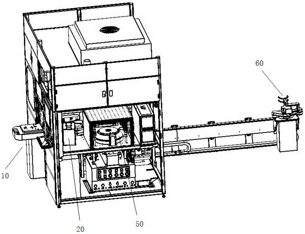
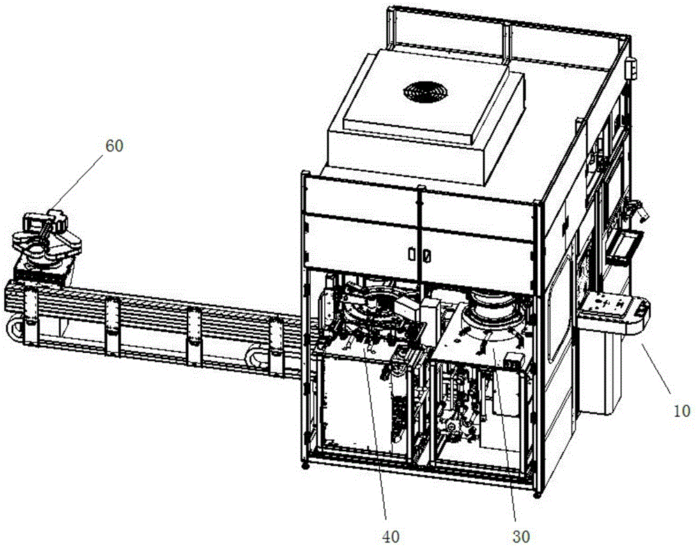
[0156] Such as figure 1 with 2 As shown, the wafer processing device includes a wafer storage box cover opening device 10 , a wafer position calibration device 20 , a wafer pre-plating processing device 30 , a wafer plating device 40 , a wafer cleaning device 50 , and a manipulator 60 . The manipulator 60 is used to transport the wafer 01 from the above-mentioned one device to the other device. The structure of manipulator 60 is prior art. The manipulator takes out the wafer from the wafer storage box, sends the wafer to the wafer electroplating pretreatment device for protection treatment, and then takes it out and sends it to the wafer electroplating device for electroplating treatment. After the electroplating is completed, the wafer is taken out by the robot and sent to the cleaning device for cleaning. After the cleaning is completed, the manipulator places the wafer on the wafer position calibration device for calibration. After the wafer position is appropriate, the ...

Embodiment 2

[0249] Different from Embodiment 1, the transmitter and receiver of the photoelectric sensor in this embodiment are located on the same side of the wafer. When the receiver can receive the beam emitted by the transmitter, it means that the beam is reflected by the wafer. When the receiver cannot receive the light beam emitted by the transmitter, it means that the light beam passes through the second through hole 011 , and the wafer 01 is located at a designated position on the support column 5 .


PUM


Abstract

The invention discloses a wafer processing unit, which is characterized by comprising a wafer electroplating pretreatment device for pre-treating wafers before electroplating, a wafer electroplating device for electroplating the wafers, a wafer cleaning device for cleaning the wafers after electroplating and a manipulator for conveying the wafers from one device to another device. According to the wafer processing unit, the wafer electroplating pretreatment device, the wafer electroplating device and the wafer cleaning device are combined organically; the wafers are conveyed by the manipulator, so that the working efficiency is improved greatly, the manpower is saved, the conveying stability of the wafers is improved, and the damage and rejection rate of the wafers is reduced.

Description

technical field [0001] The invention relates to the field of wafer manufacturing, in particular to a wafer processing device. Background technique [0002] Wafer (Wafer) refers to the silicon wafer used in the production of silicon semiconductor integrated circuits. Because of its circular shape, it is called a wafer. The processing of the wafer generally includes performing pre-plating treatment, electroplating treatment, cleaning treatment, etc. on the wafer. In the prior art, the above-mentioned processing is generally carried out in different workshops, requiring workers to transport the wafer from one workshop to another. The stability is poor, the wafer is easily damaged, and it is time-consuming, labor-intensive, inefficient, and labor-intensive. [0003] Electroplate a layer of conductive metal on the wafer, and process the conductive metal layer to make conductive lines. During the wafer production process, grooves and blind holes will be formed on the surface of ...

Claims


Application Information

Patent Timeline
IPC IPC(8): H01L21/67
CPCH01L21/288H01L21/67H01L21/67011H01L21/67023H01L21/67742H01L21/68
Inventor 王振荣黄利松刘红兵
Owner SHANGHAI SINYANG SEMICON MATERIALS
Why Eureka
Try Eureka