
Method for detecting alignment between device graph on front face of wafer and back hole on back face

A detection method and wafer technology, applied in the field of semiconductors, can solve problems such as weak penetration of infrared light on metals, blocking of deformed parts, and difficulty in detecting alignment

Active Publication Date: 2015-05-27
SEMICON MFG INT (SHANGHAI) CORP
View PDF6 Cites 7 Cited by
  • Summary
  • Abstract
  • Description
  • Claims
  • Application Information

AI Technical Summary

Problems solved by technology

However, since metal interconnection lines or other metal devices are formed on the front side S1 of the wafer 1, the penetration of infrared light to the metal is very weak, which will block the imaging of the deformation part 6 and the back hole 5, and it is difficult to detect both. Alignment in the direction perpendicular to the front of the wafer

Method used


Image

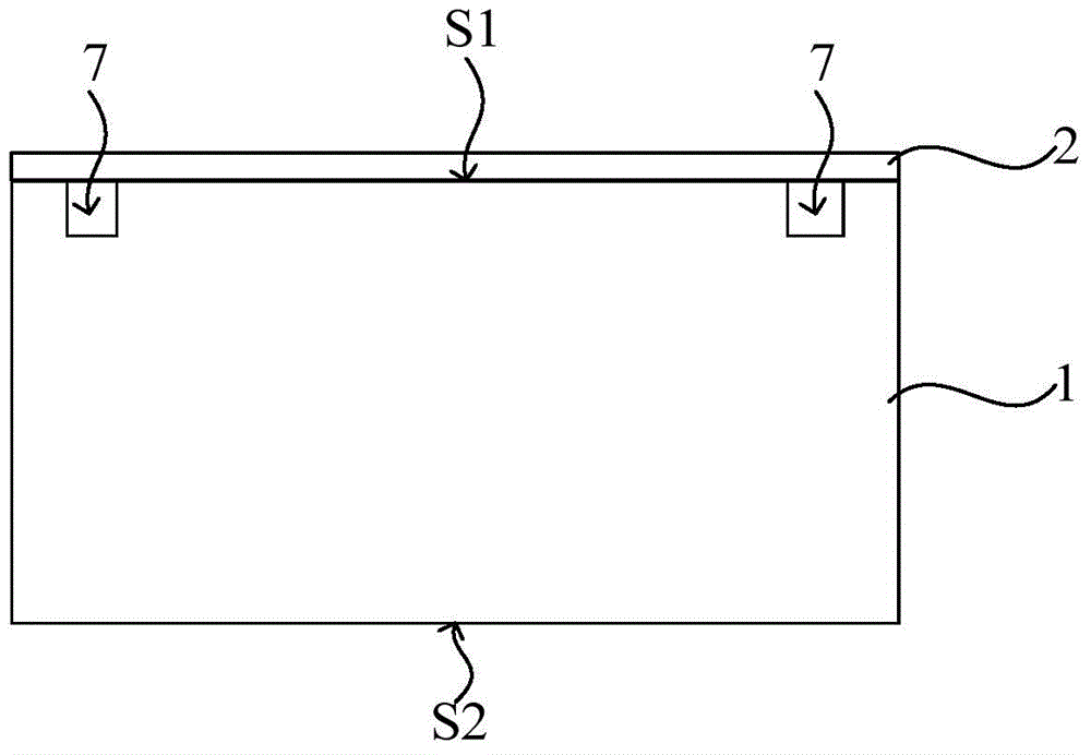
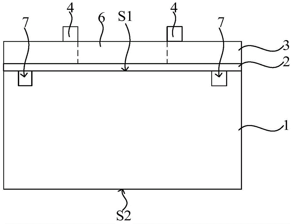
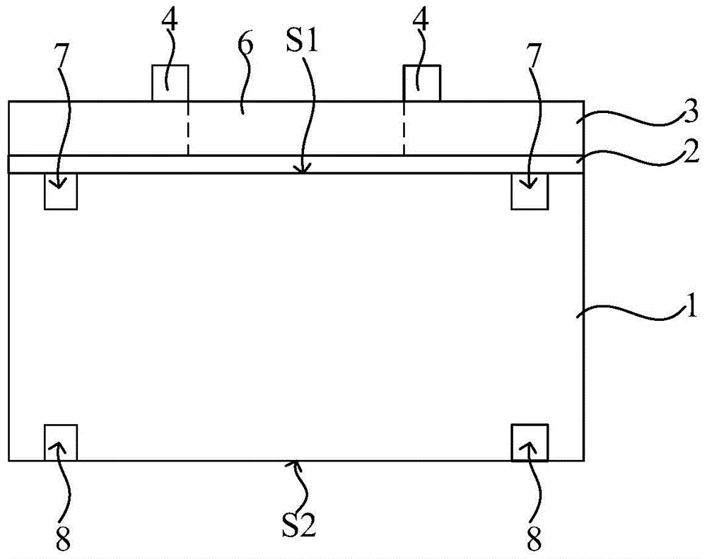
  • Method for detecting alignment between device graph on front face of wafer and back hole on back face
  • Method for detecting alignment between device graph on front face of wafer and back hole on back face
  • Method for detecting alignment between device graph on front face of wafer and back hole on back face

Examples


no. 1 example

[0062] refer to Figure 5 , a wafer 100 is provided, the wafer has a front side S1 and a back side S2, and the front side S1 and the back side S2 are parallel to each other.

[0063] In a specific embodiment, an alignment mark (not shown in the figure) may be formed on the front surface S1 of the wafer 100 , and the alignment mark plays an alignment role in the subsequent photolithography process for defining the position of the device pattern.

[0064] In a specific embodiment, the wafer 100 may be a silicon wafer, a germanium wafer, or a silicon-on-insulator wafer, etc.; or the material of the wafer 100 may also include other materials, such as Group III-V compounds such as gallium arsenide. Those skilled in the art can select wafers as required, so the types of wafers should not limit the protection scope of the present invention.

[0065] refer to Image 6 , an insulating layer 101 is formed on the front surface S1 of the wafer 100 , and the insulating layer 101 plays an...

no. 2 example

[0103] In this embodiment, refer to Figure 13 , Figure 14 , Figure 14 to correspond to Figure 13 top view, Figure 13 to correspond to Figure 14 A schematic diagram of the cross-sectional structure in the direction of BB, the detection mark 302 includes two sets of scale lines opposite to each other in a cross, namely a first set of scale lines 311 and a second set of scale lines 312 . The first set of tick marks 311 includes a plurality of first tick marks 321 spaced from each other on a straight line of the cross, and the second set of tick marks 312 includes a plurality of second tick marks separated from each other on another straight line of the cross. 322;

[0104] The intersection of the cross is defined to be within the boundary of the lower surface of the device pattern, and the boundary of the lower surface of the device pattern has two first intersections on the first set of scale lines 311 and two second intersections on the second set of scale lines 312 ...

no. 3 example

[0121] refer to Figure 18 , Figure 18In a plan view, detection marks 502 are formed on the insulating layer 501 . The detection mark 502 includes a crossed first coordinate axis 511 and a second coordinate axis 512, and the intersection of the first coordinate axis 511 and the second coordinate axis 512 is defined in the lower surface of the device pattern to be formed;

[0122] A plurality of first tick marks 521 distributed at equal intervals are set on the first coordinate axis 511 , and a plurality of second tick marks 522 distributed at equal intervals are set on the second coordinate axis 512 . The predefined first alignment position is the first coordinate of the two first intersections between the lower surface boundary of the subsequent device pattern and the first coordinate axis 511 , and the second coordinate of the two second intersections between the lower surface boundary of the device pattern and the second coordinate axis 512 . coordinate.

[0123] After ...


PUM


Abstract

The invention discloses a method for detecting alignment between a device graph on a front face of a wafer and a back hole on a back face. The method comprises steps: a wafer is provided; an insulated layer is formed on the front face of the wafer; a detection mark is formed on the upper surface of the insulated layer, and a color difference exists between the detection mark and the insulated layer; a device graph is formed on the insulated layer, and the lower surface boundary of the device graph and the detection mark have a first alignment position in the direction vertical to the front face of the wafer; a back hole is formed on the back face of the wafer; an optical microscope is used for opening observation via the back hole, a second alignment position between the bottom boundary of the back hole and the detection mark in the direction vertical to the front face of the wafer is obtained, when the second alignment position is the same as the first alignment position, the device graph is judged to be aligned with the back hole, and when the second alignment position is different from the first alignment position, the device graph is judged to be not aligned with the back hole. Irradiation of infrared light is not needed when the technical scheme of the invention is used, the optical microscope is used for direct observation, the purpose of detecting alignment between the device graph of the front face of the wafer and the back hole on the back face can be realized, and the operation is simple and easy to realize.

Description

technical field [0001] The invention relates to the technical field of semiconductors, in particular to a detection method for aligning a device pattern on the front side of a wafer with a back hole on the back side. Background technique [0002] Micro-Electro-Mechanical System (MEMS) is a tiny device that integrates micro-electronic circuits and micro-mechanical actuators. It can use sensors to receive external information, amplify the converted signals through circuit processing, and then change from actuators to mechanical operations. Execute the message command. It can be said that a MEMS is an integrated device that acquires, processes information and performs mechanical operations. [0003] Taking the MEMS pressure sensor as an example, the external pressure is received through the sensing membrane, and then converted into an electrical signal to measure the specific pressure information. Pressure sensors are divided into resistive pressure sensors and capacitive pre...

Claims


Application Information

Patent Timeline
IPC IPC(8): G01B11/00B81C1/00
Inventor 刘国安徐伟刘煊杰
Owner SEMICON MFG INT (SHANGHAI) CORP
Learn More