Method for modeling field effect transistor and circuit simulation method

A field effect transistor and transistor technology, which is applied in electrical digital data processing, special data processing applications, instruments, etc., can solve problems such as the inability to accurately describe the characteristics of field effect transistors, and achieve the effect of strong scalability and strong adaptability

Active Publication Date: 2015-05-27
SEMICON MFG INT (SHANGHAI) CORP
View PDF6 Cites 9 Cited by
  • Summary
  • Abstract
  • Description
  • Claims
  • Application Information

AI Technical Summary

Problems solved by technology

[0006] However, the field effect transistor model in the prior art simulation system based on BSIM4 etc. ignores the impact of the shallow trench isolation structure on the transistor structure: when the size of the field effect transistor is relatively large, the shallow trench isolation structure has a large impact on the field effect transisto...

Method used


Image

  • Method for modeling field effect transistor and circuit simulation method
  • Method for modeling field effect transistor and circuit simulation method
  • Method for modeling field effect transistor and circuit simulation method

Examples


Embodiment Construction

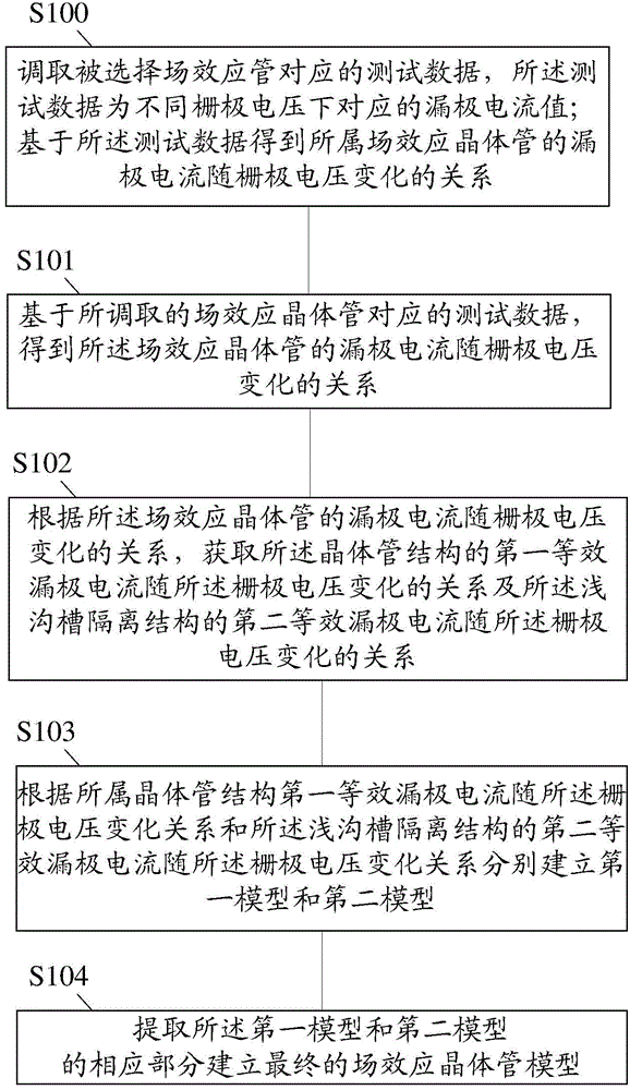
[0036] In order to make the purpose, features and effects of the present invention more obvious and understandable, the specific implementation manners of the present invention will be described in detail below in conjunction with the accompanying drawings.

[0037] Many specific details are set forth in the following description to facilitate a full understanding of the present invention, but the present invention can also be implemented in other ways than described here, so the present invention is not limited by the specific embodiments disclosed below.

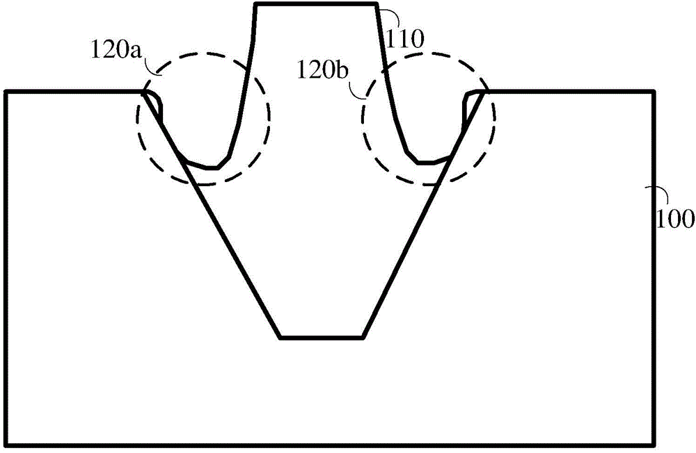
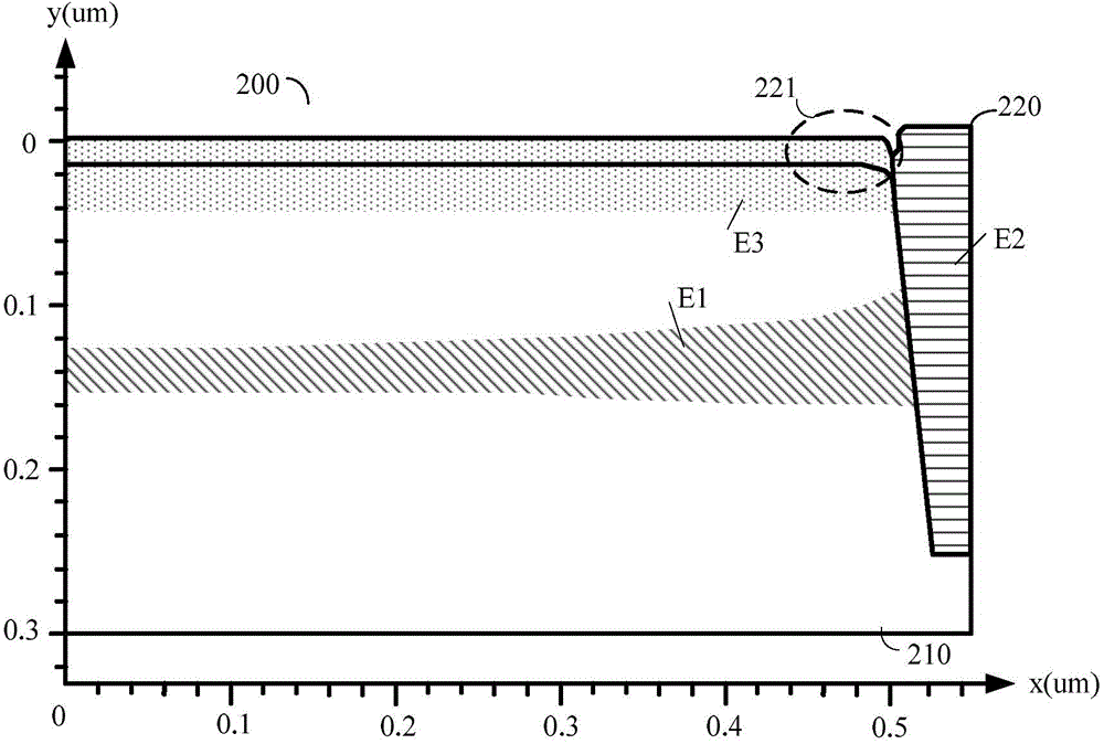
[0038] As can be seen from the background technology, the field effect transistor model of the prior art is generally provided by the integrated circuit manufacturer, and a typical field effect transistor model is BSIM4, and the field effect transistor model based on BSIM4 ignores the shallow trench isolation structure that brings the transistor impact on the structure. However, with the continuous development of the integ...


PUM

PropertyMeasurementUnit
Channel lengthaaaaaaaaaa

Abstract

The invention relates to a method for modeling a field effect transistor and a circuit simulation method. The method for modeling the field effect transistor comprises the following steps: calling gate voltage recorded by the selected field effect transistor and the corresponding drain current thereof to obtain relation for change of the drain current of the field effect transistor with the gate voltage; acquiring the relation for the change of first equivalent drain current of the transistor structure with the gate voltage and the relation for change of second equivalent drain current of a shallow trench isolating structure with the gate voltage based on the relation for the change of the drain current of the field effect transistor with the gate voltage; establishing a field effect transistor model according to the relation for the change of the first equivalent drain current of the transistor structure with the gate voltage and the relation for the change of the second equivalent drain current of the shallow trench isolating structure with the gate voltage. The accurate field effect transistor model can be established to improve the precision of circuit simulation.

Description

technical field [0001] The invention relates to the field of integrated circuit design, in particular to a method for modeling a field effect transistor and a circuit simulation method. Background technique [0002] Shallow trench isolation (STI) technology is used to realize isolation between field effect transistors (MOSFETs). The formation principle of the shallow trench isolation structure is to etch a trench on the surface of the silicon substrate corresponding to the shallow trench, and silicon dioxide (SiO 2 ) into the groove. [0003] Shallow trench isolation technology is a substitute for partial isolation silicon oxide isolation technology, and is the mainstream isolation technology for deep submicron processes. The trench of the shallow trench isolation structure has relatively steep side walls, so it has a small area, which can improve the integration degree of the field effect transistor. And because the CMP process is used in its manufacturing process, it ha...

Claims


Application Information

Patent Timeline
IPC IPC(8): G06F17/50
Inventor 魏琰董金珠
Owner SEMICON MFG INT (SHANGHAI) CORP
Why Eureka
Try Eureka