Configuration and manufacturing process of LED module

A technology for LED modules and manufacturing processes, applied in semiconductor devices, electrical components, circuits, etc., can solve problems such as difficulty in achieving high light efficiency for LED modules, poor heat dissipation of PCB substrates, and LED chip contact, and achieve good anti-failure performance. , The effect of saving metal material loss and fast processing speed

Inactive Publication Date: 2015-05-27
莆田康布斯光电科技有限公司
View PDF4 Cites 3 Cited by
  • Summary
  • Abstract
  • Description
  • Claims
  • Application Information

AI Technical Summary

Problems solved by technology

[0005] Aiming at the problems of poor heat dissipation of the PCB substrate in the existing LED module structure and production process, the contact and thermal resistance caused by LED chip welding, and the shortc...

Method used


Image

  • Configuration and manufacturing process of LED module
  • Configuration and manufacturing process of LED module
  • Configuration and manufacturing process of LED module

Examples


Embodiment 1

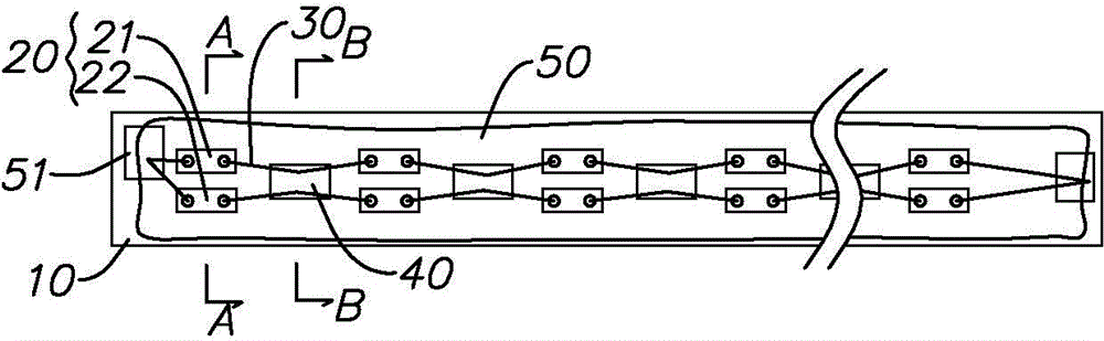
[0044] Figure 1 to Figure 3 Shows a structural diagram of an embodiment of the present invention.

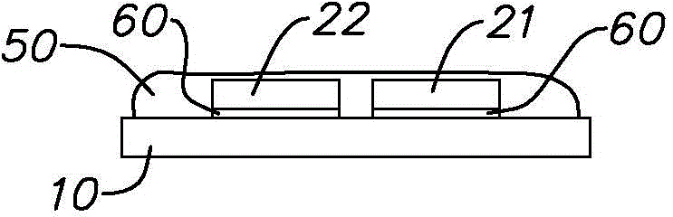
[0045] It has a mirror substrate 10, which is made of metal or ceramic material and has a small thermal resistance. A number of LED chips, including 21 and 22, are fixed on the upper surface of the substrate 10 through an insulating glue layer 60; two groups of LED chips form an LED pair 20, such as the LED chips 21 and 22 shown in this figure. An LED pair, the LED pair is a unit, along the length of the substrate 10, namely figure 1 The LED chips 21 and 22 are arranged in a direction from left to right, and the electrodes of the LED chips 21 and 22 face upward. The substrate electrode 51 is also fixed on the upper surface of the substrate 10 with an insulating glue layer 60.

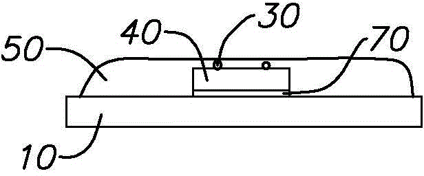
[0046] The bonding wire 30 is used as the main connection for constructing the electrical topology of the LED chip. It is connected to the substrate electrode 51 and the electrode of the LED chip including 2...

Embodiment 2

[0059] Such as Figure 4 to Figure 7 As shown, the schematic diagram of the second embodiment of the present invention.

[0060] This solution has a thermally conductive substrate 10, the substrate 10 is made of aluminum material with a high polish on the upper surface, and has the characteristics of high reflectivity and high thermal conductivity. Multiple LED chips, including 21 and 22, are fixed on the upper surface of the substrate 10 through an insulating glue layer 60; two LED chips form a pair of LEDs, such as the LED chips 21 and 22 shown in this figure, which constitute An LED pair 20, the LED pair 20 is a unit, along the length of the substrate 10, namely figure 1 The LED chips 21 and 22 are arranged in a direction from left to right, and the electrodes of the LED chips 21 and 22 face upward. The substrate electrode 51 is also fixed on the upper surface of the substrate 10 with an insulating glue layer 60.

[0061] The bonding wire 30 is used as the main connection for ...


PUM


Abstract

The invention discloses a configuration and a manufacturing process of an LED module. The manufacturing process is characterized by comprising the following steps: LED chips are fixed on the upper surface of a substrate by an insulating adhesive layer; two LED chips form a group and form an LED pair, electrode surfaces are upward; electrodes of the substrate are fixed on the upper surface of the substrate by the insulating adhesive layer; bonding wires are bonded to the electrodes of the substrate and the electrodes of the LED chip; a parallel connection part is arranged between every two adjacent LED pairs, and the bonding wire is led out from the electrodes of each LED chip in the LED pair and then is connected to the parallel connection part, so that the LED pairs become parallel connection units electrically connected in parallel; all parallel connection units are connected in series by the parallel connection part to form an LED string; finally, a phosphor layer is coated to cover the LED chips, the bonding wires and the insulating adhesive layer. According to the invention, all insulating layers and welding points of the substrate body are omitted; the thermal resistance is low; the uneven heat conduction caused by the welding process/configuration is further avoided; the LED chips are simple in fixing process and structure, and high in processing speed.

Description

Technical field [0001] The invention relates to the structure of an LED module and its manufacturing process. Background technique [0002] LED is becoming more and more popular in the field of lighting activities, so the demand for its products is also increasing, from concentrating lamps to the general lighting field including various flood lighting, a variety of LED modules have also emerged. Its purpose is to replace traditional light sources such as incandescent lamps and fluorescent lamps that have been widely used in lamp structures, so as to obtain even better lighting performance. [0003] Taking into account the characteristics of LED light sources, when a large area of ​​luminous body needs to be realized, a huge number of LED chip particles will inevitably be mounted on various forms of substrates, such as long strips of light, so that it has a uniform The light-emitting surface, on the one hand, can obtain a better heat dissipation effect, and on the other hand, it mu...

Claims


Application Information

Patent Timeline
IPC IPC(8): H01L25/13H01L33/64H01L33/62
CPCH01L24/48H01L2224/48091H01L2224/48137H01L2224/48227H01L2224/49113H01L2224/4917H01L2224/73265H01L2224/8592H01L2224/48998H01L2924/181H01L2224/49H01L2224/48H01L2924/00014H01L2924/00012
Inventor 吴鼎鼎
Owner 莆田康布斯光电科技有限公司
Why Eureka
Try Eureka