Printed circuit board and method for manufacturing printed circuit board

A technology for printed circuit boards and sub-boards, applied in multilayer circuit manufacturing, printed circuit components, and electrical connection formation of printed components, etc. It can solve hole wall corrosion, affect the electrical performance of printed circuit boards, and easily enter blind holes, etc. question

Active Publication Date: 2018-09-21
HUAWEI TECH CO LTD
View PDF5 Cites 0 Cited by
  • Summary
  • Abstract
  • Description
  • Claims
  • Application Information

AI Technical Summary

Problems solved by technology

[0004] In the prior art, pre-opened prepreg combined with copper foil is used to protect the crimped blind hole of the sub-board against infiltration. The prepreg has certain fluidity at high temperature. Therefore, the fluid material constituting the prepreg can easily enter the blind hole. , corrodes the hole wall and affects the electrical performance of the entire printed circuit board

Method used


Image

  • Printed circuit board and method for manufacturing printed circuit board
  • Printed circuit board and method for manufacturing printed circuit board
  • Printed circuit board and method for manufacturing printed circuit board

Examples


Embodiment Construction

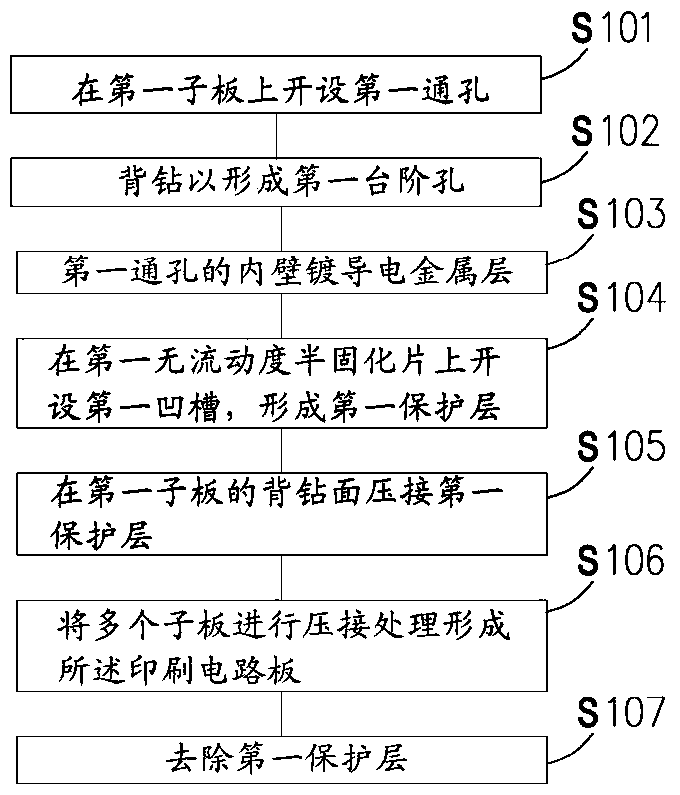
[0067] The following will clearly and completely describe the technical solutions in the embodiments of the present invention with reference to the accompanying drawings in the embodiments of the present invention. Obviously, the described embodiments are only some, not all, embodiments of the present invention. Based on the embodiments of the present invention, all other embodiments obtained by persons of ordinary skill in the art without creative efforts fall within the protection scope of the present invention.

[0068] see Figure 1 to Figure 7 , an embodiment of the present invention provides a method for manufacturing a printed circuit board, comprising the following steps:

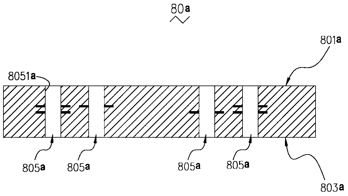
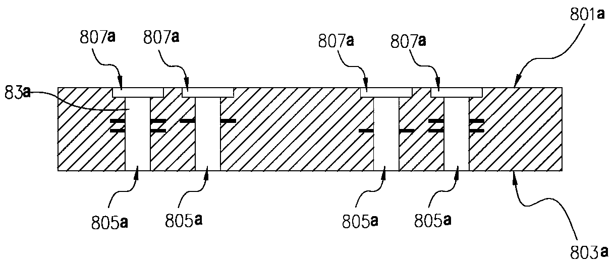
[0069] Step S101, such as figure 2 As shown, at least one first through hole 805a is opened on the first sub-board 80a, and the first sub-board 80a is provided with a back-drilling surface 801a and a crimping surface 803a disposed opposite to each other. The first through hole 805a passes through...


PUM


Abstract

The invention provides a printed circuit board. The printed circuit board comprises multiple daughter boards, wherein the daughter boards comprise a first daughter board located on the outermost side of the printed circuit board; at least one first through hole is formed in the first daughter board and penetrates through back drilling surface and a compression joint surface of the first daughter board; the wall of the first through hole is plated with a conductive metal layer; a first step hole is formed in the first daughter board in a back drilling manner and is communicated with the first through hole; the projection of the first step hole on the back drilling surface of the first daughter board covers the projection of the first through hole on the back drilling surface of the first daughter board; the first step hole is separated from other holes formed in the first daughter board. The invention further provides a manufacturing method of the printed circuit board. According to the printed circuit board and the method, the step hole is formed, so that accommodation space for accommodating a fluid is formed, and the fluid can be prevented from flowing into a blind hole of the printed circuit board.

Description

technical field [0001] The invention relates to the field of electronic devices, in particular to a printed circuit board and a method for manufacturing the printed circuit board. Background technique [0002] With the development of science and technology, people have higher and higher requirements for the integration of integrated circuit boards. Ordinary single-sided crimping cannot meet the needs of system capacity. Double-sided crimping blind hole design is adopted, that is, two sub-boards are superimposed to form a mother board. Board structure, which can realize double-sided crimping and expand the capacity of the backplane. In addition, the demand for high-speed performance makes the density of the crimping connectors smaller and smaller, and the pitch of the crimping blind holes on the corresponding printed circuit board is getting smaller and smaller. [0003] When crimping the sub-board to form the mother board or processing the through-hole of the mother board, ...

Claims


Application Information

Patent Timeline
Patent Type & Authority Patents(China)
IPC IPC(8): H05K1/02H05K1/11H05K3/42H05K3/46
Inventor 蔡黎刘山当李志海高峰
Owner HUAWEI TECH CO LTD
Why Eureka
Try Eureka