Accelerating simulated annealing method for integrated circuit layout

A technology of simulated annealing and integrated circuits, applied in the direction of electrical digital data processing, special data processing applications, instruments, etc., can solve the problems of reducing layout time and unacceptable algorithm running time, so as to reduce layout time and reduce algorithm running time, reducing the effect of invalid moves

Active Publication Date: 2015-06-03
INST OF ELECTRONICS CHINESE ACAD OF SCI
View PDF2 Cites 2 Cited by
  • Summary
  • Abstract
  • Description
  • Claims
  • Application Information

AI Technical Summary

Problems solved by technology

[0009] In order to overcome the defective of prior art, technical scheme simulated annealing algorithm of the present invention is widely used to solve the layout problem of FPGA, but along with the increase of FPGA chip capacity, the running time of algorithm becomes unacceptable; For this reason, the purpose of the present invention It is to propose an acceleration method of simulated annealing algorithm, and use it in the layout of FPGA, reduce the layout time, and keep the wiring length and frequency of the circuit within the specified range

Method used


Image

  • Accelerating simulated annealing method for integrated circuit layout
  • Accelerating simulated annealing method for integrated circuit layout
  • Accelerating simulated annealing method for integrated circuit layout

Examples


Embodiment Construction

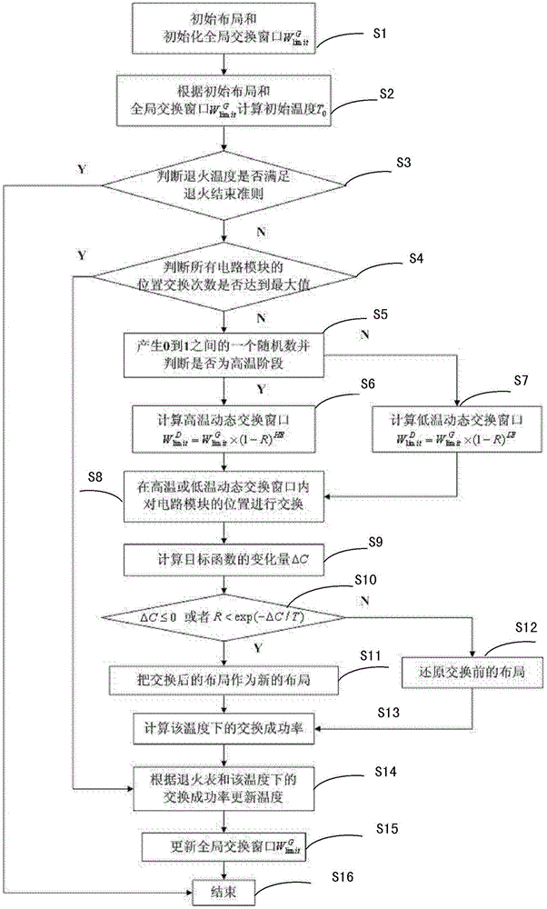
[0018] In order to make the object, technical solution and advantages of the present invention clearer, the present invention will be described in further detail below in conjunction with specific embodiments and with reference to the accompanying drawings.

[0019] An accelerated simulated annealing (SA) method for integrated circuit layout of the present invention changes the calculation method of the exchange window in the simulated annealing method, so that the exchange window is not only determined by the exchange success rate at the previous temperature, but also related to It is related to a random number R that determines whether a certain exchange is accepted, so that the window size of each exchange changes dynamically with the random number R. In addition, different dynamic exchange window adjustment strategies are adopted for the high-temperature and low-temperature stages of annealing, that is, the dynamic exchange window is narrowed in the high-temperature stage; ...


PUM


Abstract

The invention relates to an accelerating simulated annealing method for integrated circuit layout. The method includes the steps of changing the size of each dynamic exchange window of a circuit module included in an integrated circuit; according to exchange success rate at former temperature and a random number for determining whether or not certain exchange is accepted, determining the sizes of the dynamic exchange windows, and allowing the size of each dynamic exchange window engaging in exchanging to dynamically change with the random number; applying different dynamic exchange window regulating strategies according to annealing high-temperature and low-temperature phases, thus allowing a whole simulated annealing process, from high temperature to low temperature, for the layout of the circuit module.

Description

technical field [0001] The invention relates to optimizing the layout of a field programmable logic chip (FPGA), reducing the layout time, while keeping the wiring length and frequency of the circuit within a prescribed range. Background technique [0002] (1) With the continuous shrinking of integrated circuit process nodes, the number of look-up table modules (Look Up Table-LUT) included in modern field programmable logic chips (Field Programmable Gate Array-FPGA) has reached the order of millions, and embedded Many hard modules, such as digital signal processing module (Digital Signal Process-DSP), random storage module (Random Access Memory-RAM) and so on. Due to the increasing complexity of heterogeneous FPGAs, the compilation time of computer-aided design (CAD) tools is getting longer and longer, and layout is one of the most time-consuming steps in the entire compilation flow of FPGAs. The negative effect is that digital circuit design Or the prolongation of the desi...

Claims


Application Information

Patent Timeline
Patent Type & Authority Applications(China)
IPC IPC(8): G06F17/50
Inventor 杨海钢黄俊英林郁崔秀海罗杨王飞
Owner INST OF ELECTRONICS CHINESE ACAD OF SCI
Why Eureka
Try Eureka