Diode structure for reducing anode hole injection

A hole injection and diode technology, applied in electrical components, circuits, semiconductor devices, etc., can solve problems such as large dynamic loss, increased leakage, and increased contact resistance, achieving compact structure, reducing dynamic loss, and reducing hole injection. amount of effect

Inactive Publication Date: 2015-06-03
JIANGSU CAS IGBT TECHNOLOGY CO LTD
View PDF4 Cites 0 Cited by
  • Summary
  • Abstract
  • Description
  • Claims
  • Application Information

AI Technical Summary

Problems solved by technology

When working, a voltage is applied through the anode metal 1 and the cathode metal 4 to form a forward-conducting PN junction, but the existing diode structure has the disadvantage of large dynamic loss
At present, in order to reduce the dynamic loss of the diode, the loss can be reduced by reducing the concentration of the P conductive region 2 or by introducing lifetime control (heavy metal or electron beam radiation), but reducing the concentration of the P conductive region 2 will lead to a larger contact resistance, and then lead to increased loss; and when the loss is reduced by introducing life control, it is easy to cause a large increase in leakage

Method used


Image

  • Diode structure for reducing anode hole injection
  • Diode structure for reducing anode hole injection
  • Diode structure for reducing anode hole injection

Examples


Embodiment Construction

[0012] The present invention will be further described below in conjunction with specific drawings and embodiments.

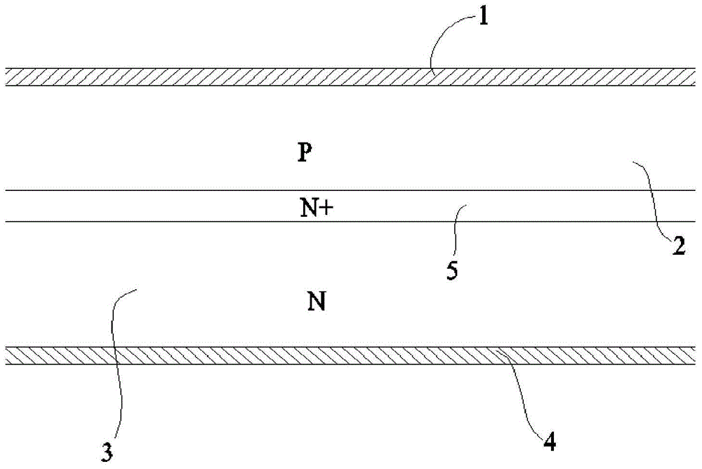
[0013] Such as figure 2 As shown: in order to effectively reduce the dynamic loss of the diode by reducing the anode hole injection, the present invention includes a semiconductor substrate, which includes a P conductive region 2 and an N conductive region 3 for forming a PN junction; in the P An N+ region 5 with a doping concentration higher than that of the N conductive region 3 is disposed between the conductive region 2 and the N conductive region 3 .

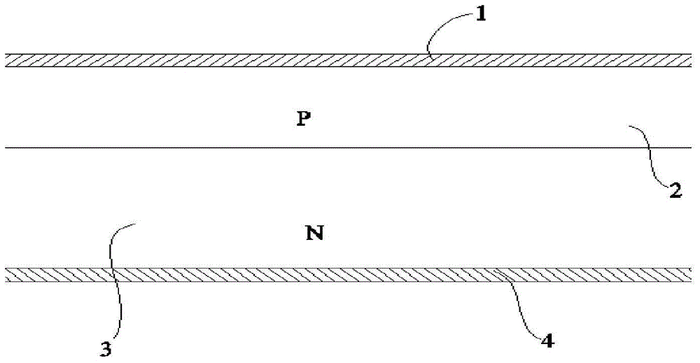
[0014] The semiconductor substrate includes a silicon substrate. An anode metal 1 for ohmic contact with the P conductive region 2 is arranged on the front of the semiconductor substrate, and a cathode metal 4 for ohmic contact with the N conductive region 3 is arranged on the back of the semiconductor substrate.

[0015] Specifically, the material of the semiconductor substrate may be silicon, the upper s...


PUM


Abstract

The invention relates to a diode structure, in particular to a diode structure for reducing the anode hole injection and belongs to the technical field of semiconductor diodes. According to the technical scheme provided by the invention, the diode structure for reducing the anode hole injection comprises a semiconductor substrate, wherein a P conducting region and an N conducting region for forming a PN junction are arranged in the semiconductor substrate; an N+region of which the doping concentration is larger than that of the N conducting region is arranged between the P conducting region and the N conducting region. According to the diode structure, as the N+region is arranged between the P conducting region and the N conducting region, and the doping concentration of the N+region is larger than that of the N conducting region, in combination with the N+region and a hole in the P conducting region, the hole injection quantity in the N conducting region is reduced, so that the dynamic loss of a diode can be effectively reduced; the diode structure is compact, safe and reliable.

Description

technical field [0001] The invention relates to a diode structure, in particular to a diode structure for reducing anode hole injection, and belongs to the technical field of semiconductor diodes. Background technique [0002] Such as figure 1 Shown is the structure of the existing diode, including the P conductive region 2 and the N conductive region 3 for forming a PN junction, the P conductive region 2 is connected to the N conductive region 3, and the anode metal 1 is arranged on the P conductive region 2, and The cathode metal 4 is arranged on the N conductive region 3 , the anode metal 1 is in ohmic contact with the P conductive region 2 , and the cathode metal 4 is in ohmic contact with the N conductive region 3 . During operation, a voltage is applied through the anode metal 1 and the cathode metal 4 to form a forward conduction PN junction, but the existing diode structure has the disadvantage of large dynamic loss. At present, in order to reduce the dynamic loss ...

Claims


Application Information

Patent Timeline
Patent Type & Authority Applications(China)
IPC IPC(8): H01L29/861H01L29/02H01L29/45
CPCH01L29/861H01L29/0657H01L29/456
Inventor 程炜涛
Owner JIANGSU CAS IGBT TECHNOLOGY CO LTD
Why Eureka
Try Eureka