Detection substrate, preparation method thereof, and detector
A technology for detecting substrates and substrate substrates, which is applied in the field of detection, can solve problems such as the detection substrate’s reduced utilization efficiency of light, and achieve the effect of improving utilization efficiency
- Summary
- Abstract
- Description
- Claims
- Application Information
AI Technical Summary
Problems solved by technology
Method used
Image


Examples
Embodiment 2
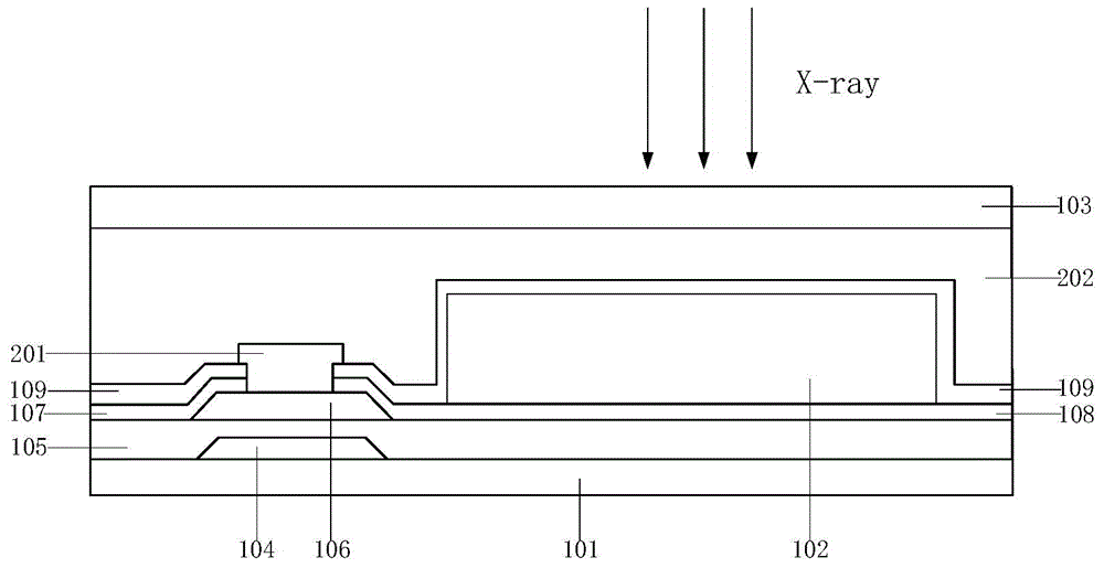
[0033] image 3 It is a schematic structural diagram of another detection substrate provided in Embodiment 2 of the present invention. Such as image 3 As shown, the detection substrate includes a base substrate 101, a thin film transistor, a PIN photodiode and a scintillation layer 103, and the thin film transistor includes a gate 104, an active layer 106, a source 107 and a drain 108, and the thin film The transistor and the PIN photodiode are disposed on the first surface of the base substrate 101 , and the scintillation layer 103 is disposed on the second surface of the base substrate 101 . It should be noted that, in this embodiment, the drain 108 of the thin film transistor is equivalent to the anode of the PIN photodiode.
[0034] In practical application, the scintillator layer 103 is made of scintillator material, for example, Gd 2 o 2 S, CsI or HgI composition. The function of the scintillation layer 103 is to convert the absorbed high-energy particles or rays i...
Embodiment 3
[0042] This embodiment provides a detector, including the detection substrate provided in Embodiment 1 or Embodiment 2 above. Regarding the specific content of the detection substrate, reference may be made to the description in the first embodiment or the second embodiment above, which will not be repeated here.
[0043] In the detector provided in this embodiment, the detection substrate includes a base substrate, a thin film transistor, a PIN photodiode, and a scintillation layer, and the thin film transistor and the PIN photodiode are arranged on the first surface of the base substrate, The scintillation layer is disposed on the second surface of the base substrate. The X-rays directly irradiate the PIN photodiode after passing through the base substrate with high transmittance, so as to avoid weakening of the light intensity irradiated to the PIN photodiode, thereby improving the light utilization efficiency of the detection substrate.
Embodiment 4
[0045] Figure 4 It is a flow chart of a method for preparing a detection substrate provided in Embodiment 4 of the present invention. Such as Figure 4 Shown, described preparation method comprises:
[0046] Step 4001, forming a thin film transistor and a PIN photodiode on the first surface of the substrate, the thin film transistor including a gate, an active layer, a source and a drain.
[0047] Step 4002, forming a scintillation layer on the second surface of the base substrate.
[0048] see figure 2 , the detection substrate includes a base substrate 101, a thin film transistor, a PIN photodiode and a scintillation layer 103, the thin film transistor includes a gate 104, an active layer 106, a source 107 and a drain 108, and the thin film transistor and The PIN photodiode is disposed on the first surface of the base substrate 101 , and the scintillation layer 103 is disposed on the second surface of the base substrate 101 . It should be noted that, in this embodimen...
PUM
 Abstract
Description
Claims
Application Information
 - R&D
- Intellectual Property
- Life Sciences
- Materials
- Tech Scout
- Unparalleled Data Quality
- Higher Quality Content
- 60% Fewer Hallucinations
Browse by: Latest US Patents, China's latest patents, Technical Efficacy Thesaurus, Application Domain, Technology Topic, Popular Technical Reports.
© 2025 PatSnap. All rights reserved.Legal|Privacy policy|Modern Slavery Act Transparency Statement|Sitemap|About US| Contact US: help@patsnap.com