GaN-based high-voltage direct-current LED insulation isolating process

An insulation isolation, high voltage DC technology, applied in electrical components, electrical solid devices, circuits, etc., can solve problems such as increased equipment cost, disadvantageous compression packaging material cost, complex process, etc., to reduce the injection current density and reduce the loss of light-emitting area. , The effect of smoothing the sidewall surface

Inactive Publication Date: 2015-06-03
JIANGSU XINGUANGLIAN SEMICON
View PDF4 Cites 14 Cited by
  • Summary
  • Abstract
  • Description
  • Claims
  • Application Information

AI Technical Summary

Problems solved by technology

Considering that the current mainstream COB-LED is composed of a single LED chip, it also has the following shortcomings: 1), each LED needs to be bonded and interconnected one by one, the production efficiency is relatively low, the equipment cost is increased, and the product yield is affected; 2) The arrangement of LED grains should not be too compact, which is not conducive to reducing the cost of packaging materials
[0004] Compared with traditional LEDs, the process of making GaN-based high-voltage DC LEDs is more complicated, and the insulation and isolation of LED subunits is the difficulty.
The usual method is to use dry etching to remove the excess epitaxial layer between the subunits. Although this method can obtain insulation isolation, it is not an ideal method from the perspective of actual production, because the entire GaN-based LED epitaxy The thickness of the layer is generally around 6-10 μm (thicker μ-GaN needs to be grown to obtain better growth quality), which is bound to greatly increase the etching time and require additional deposition of SiO 2 Thick masks greatly occupy the production capacity of ICP and PECVD equipment; in addition, there are certain process uncertainties in the dry deep etching of GaN-based epitaxial layers, such as rough sidewall morphology, which may easily lead to failure of interconnect electrode adhesion; etching trenches may There are conductive substances remaining, resulting in abnormal photoelectric characteristics of the device
In order to avoid the above potential problems as much as possible, the groove width is generally relaxed, so that the device loses part of the light-emitting area. Therefore, it is urgent to develop a new GaN-based high-voltage DC LED insulation isolation processing method.

Method used


Image

  • GaN-based high-voltage direct-current LED insulation isolating process
  • GaN-based high-voltage direct-current LED insulation isolating process
  • GaN-based high-voltage direct-current LED insulation isolating process

Examples


Embodiment Construction

[0039] The present invention will be further described below in conjunction with specific drawings and embodiments.

[0040] In order to effectively improve the insulation and isolation performance between multiple LED sub-units, greatly improve production efficiency, ensure production yield, and improve the performance of high-voltage DC LEDs, the insulation and isolation process of the present invention includes the following steps:

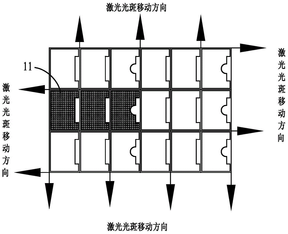
[0041] a. Provide a sapphire substrate 5 grown with an epitaxial layer 20, and define the MESA pattern of the LED subunit 11 on the epitaxial layer 20;

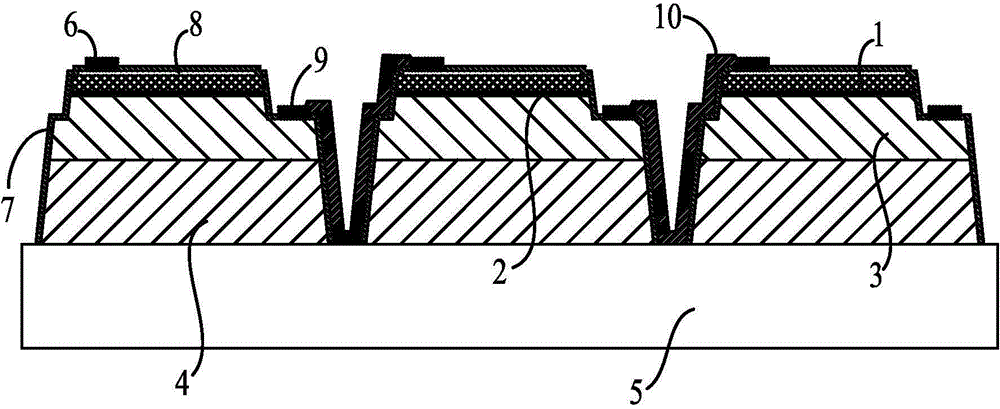
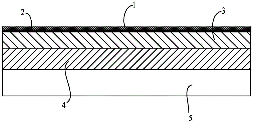
[0042] like image 3 and Figure 4 As shown, the epitaxial layer 20 includes the μ-GaN layer 4 grown on the sapphire substrate 5, the N-GaN layer 3 grown on the μ-GaN layer 4, the N-GaN layer 3 grown on the N-GaN layer 3 The multi-quantum well 2 and the P-GaN layer 1 grown on the multi-quantum well 2.

[0043] In order to define the MESA pattern of the LED subunit 11 on the epitaxial layer ...


PUM


Abstract

The invention relates to a GaN-based high-voltage direct-current LED insulation isolating process. The process comprises the following steps: a, providing a sapphire substrate on which an epitaxial layer grows, and defining MESA patterns of LED subunits on the epitaxial layer; b, performing dry etching on the epitaxial layer by utilizing the MESA patterns to obtain MESA table boards of the LED subunits; c, depositing etching mask layers, wherein the etching mask layers cover the MESA table boards; d, ablating the epitaxial layer between the MESA table boards of every adjacent two LED subunits and the etching mask layers by utilizing pulse laser spots of a laser so as to form an isolation groove between every adjacent two MESA table boards of the LED subunits, and isolate every adjacent two LED subunits each other through the corresponding isolation groove; e, removing impurities generated by the ablation of the pulse laser spots in each isolation groove so as to smoothen the side wall surface of each isolation groove; f, removing the etching mask layers. According to the process, the insulation isolating performance between adjacent two LED subunits can be effectively improved; the production efficiency is greatly improved; the yield is ensured; the performance of a high-voltage direct-current LED is improved; the process is safe and reliable.

Description

technical field [0001] The invention relates to an isolation process, in particular to a GaN-based high-voltage DC LED insulation isolation process, belonging to the technical field of DC high-voltage LED manufacturing process. Background technique [0002] The key to the popularization of LED lighting lies in the development of high-efficiency, low-cost device structures. The integrated packaging (COB-LED) that has appeared in recent years is just one of the potential device structures. COB-LED is composed of multiple LEDs fixed on a large-area heat dissipation substrate (heat sink) and connected in series and parallel. COB-LED can significantly improve the heat dissipation problem, use low current drive to give full play to the advantages of high light efficiency of LED, and greatly save packaging cost compared with single LED packaging. Considering that the current mainstream COB-LED is composed of a single LED chip, it also has the following shortcomings: 1), each LED n...

Claims


Application Information

Patent Timeline
Patent Type & Authority Applications(China)
IPC IPC(8): H01L33/00H01L27/15
CPCH01L33/005H01L21/76H01L27/153
Inventor 李睿
Owner JIANGSU XINGUANGLIAN SEMICON
Why Eureka
Try Eureka