Reflective layer structure of a light emitting diode

A technology of light-emitting diodes and reflective layers, which is applied in the direction of electrical components, circuits, semiconductor devices, etc., can solve the problems of unstable mirror structure, easy to be oxidized, and low reflectivity, and achieve simple structure, avoid falling off, and high reflectivity Effect

Active Publication Date: 2018-03-20
EPILIGHT TECH
View PDF3 Cites 0 Cited by
  • Summary
  • Abstract
  • Description
  • Claims
  • Application Information

AI Technical Summary

Problems solved by technology

[0006] In view of the above-mentioned shortcomings of the prior art, the purpose of the present invention is to provide a light-emitting diode reflector structure, which is used to solve the problem t

Method used


Image

  • Reflective layer structure of a light emitting diode
  • Reflective layer structure of a light emitting diode
  • Reflective layer structure of a light emitting diode

Examples


Example Embodiment

[0037] Example 1

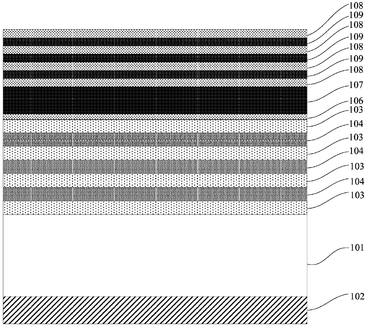
[0038] Such as figure 1 As shown, this embodiment provides a reflective layer structure of a light emitting diode, which at least includes:

[0039] Dielectric stack, including alternate stacks of SiO 2 Layer 103 and Ti 3 O 5 Layer 104, wherein the bottom layer of the dielectric stack is SiO 2 Layer 103;

[0040] The middle Ni layer 106 is bonded to the surface of the dielectric laminate;

[0041] The Ag reflective layer 107 is bonded to the surface of the intermediate Ni layer 106;

[0042] The metal stack includes Ni layer 108 and Ag layer 109 alternately stacked, wherein the top layer of the metal stack is Ni layer 108.

[0043] The dielectric stack is combined with the back surface of the thinned sapphire substrate 101 of the light emitting diode, and a light emitting epitaxial structure 102 is prepared on the front surface of the sapphire substrate 101. The dielectric stack includes a plurality of alternately stacked SiO 2 Layer 103 and Ti 3 O 5 Layer 104, and ea...

Example Embodiment

[0048] Example 2

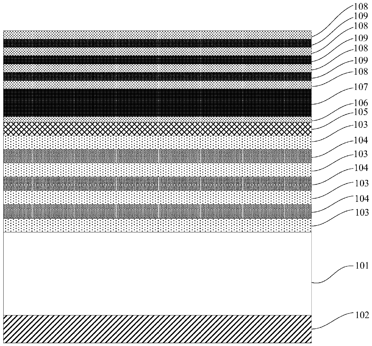
[0049] Such as figure 2 As shown, this embodiment provides a reflective layer structure of a light emitting diode, the basic structure of which is as in embodiment 1, wherein the dielectric stack also includes SiO bonded to the top layer 2 Al on the surface of layer 103 2 O 3 Layer 105, the Al 2 O 3 The thickness of the layer 105 is not greater than 1 micron, and within this thickness range, the reflection effect of the dielectric stack will not be reduced.

[0050] The Al 2 O 3 Layer 105, which is combined with the SiO 2 The layer 103 has a higher bonding strength, and the bonding strength with the middle Ni layer 106 is higher than that of SiO 2 The layer 103 is higher, so the SiO on the top layer 2 Layer 103 first prepare a layer of Al 2 O 3 Compared with Embodiment 1, the layer 105 can make the Ag reflective layer 107 stronger.

Example Embodiment

[0051] Example 3

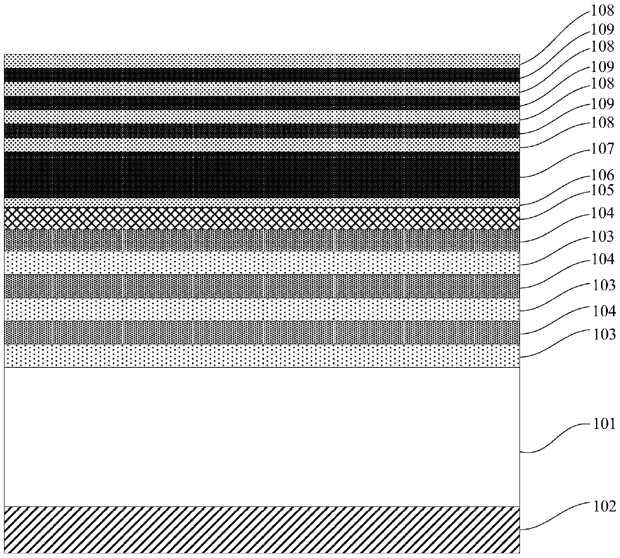
[0052] Such as image 3 As shown, this embodiment provides a reflective layer structure of a light emitting diode, the basic structure of which is as in embodiment 1, wherein the top layer of the dielectric stack is Ti 3 O 5 Layer 104, and the dielectric stack also includes Ti bonded to the top layer 3 O 5 Al on the surface of layer 104 2 O 3 Layer 105, and the Al 2 O 3 The thickness of layer 105 is not greater than 1 micron.

[0053] The Al 2 O 3 Layer 105 with the Ti 3 O 5 The layer 104 has a higher bonding strength, and the bonding strength with the middle Ni layer 106 is higher than that of SiO 2 The layer 103 is higher, so the Ti 3 O 5 Layer 104 first prepare a layer of Al 2 O 3 Layer 105, used to replace SiO 2 Compared with Embodiment 1, the layer 103 can make the Ag reflective layer 107 stronger.

[0054] As described above, the present invention provides a reflective layer structure of a light emitting diode, which at least includes: a dielectric stack inclu...


PUM

PropertyMeasurementUnit
Thicknessaaaaaaaaaa
Thicknessaaaaaaaaaa
Thicknessaaaaaaaaaa

Abstract

The invention provides a reflecting layer structure of a light-emitting diode. The reflecting layer structure at least comprises a medium laminate, an intermediate Ni layer, an Ag reflecting layer and a metal laminate, wherein the medium laminate comprises a SiO2 layer and Ti3O5 layers, which are laminated alternately; a bottom layer of the medium laminate is the SiO2 layer; the intermediate Ni layer is combined on the surface of the medium laminate; the Ag reflecting layer is combined on the surface of the intermediate Ni layer; the metal laminate comprises Ni layers and Ag layers, which are laminated alternately; a top layer of the metal laminate is the Ni layer. The reflecting layer structure has the following beneficial effects that the SiO2 layers and the Ti3O5 layers which are laminated alternately of the reflecting layer structure have a better reflection effect compared with that of a common medium layer; the ultrathin intermediate Ni layer is adopted, the reflectivity is not reduced, the adhesion performance between the Ag reflecting layer and the medium laminate is also improved greatly, and the Ag reflecting layer is prevented from falling off; the Ni layers and the Ag layers which are laminated alternately can protect the Ag reflecting layer from being oxidized quite well, and the stability and the reflectivity of the reflecting layer structure are guaranteed.

Description

technical field [0001] The invention relates to a structure of a light emitting diode, in particular to a reflective layer structure of a light emitting diode. Background technique [0002] With the rapid development of science and technology, people have more and more choices for lighting devices in life. From traditional tungsten filament bulbs to fluorescent lamps, lighting devices are constantly being introduced. In recent years, light-emitting diodes (Light Emitting Diode, LED) have developed rapidly. Due to their advantages such as small size, high efficiency, long life, and stable photoelectric characteristics, light-emitting diodes are gradually widely used in household appliances, computer screens, mobile phones, lighting equipment, Fields such as medical equipment or traffic signals. [0003] The luminous efficiency of LED is limited by the external quantum efficiency, and the external quantum efficiency is determined by the internal quantum efficiency and light e...

Claims


Application Information

Patent Timeline
IPC IPC(8): H01L33/46
CPCH01L33/46
Inventor 朱广敏郝茂盛齐胜利邢志刚袁根如
Owner EPILIGHT TECH
Why Eureka
Try Eureka