A kind of thick copper circuit board processing method

A processing method and circuit board technology, which is applied in printed circuit, printed circuit, printed circuit manufacturing, etc., to achieve the effect of small hardness increase, improved thickness uniformity, and avoid delamination or board explosion

Active Publication Date: 2017-12-12
SHENNAN CIRCUITS
View PDF5 Cites 0 Cited by
  • Summary
  • Abstract
  • Description
  • Claims
  • Application Information

AI Technical Summary

Problems solved by technology

[0006] The embodiment of the present invention provides a thick copper circuit board processing method to solve the above-mentioned problems existing in the existing thick copper circuit board pressing process

Method used


Image

  • A kind of thick copper circuit board processing method
  • A kind of thick copper circuit board processing method
  • A kind of thick copper circuit board processing method

Examples


Embodiment 1

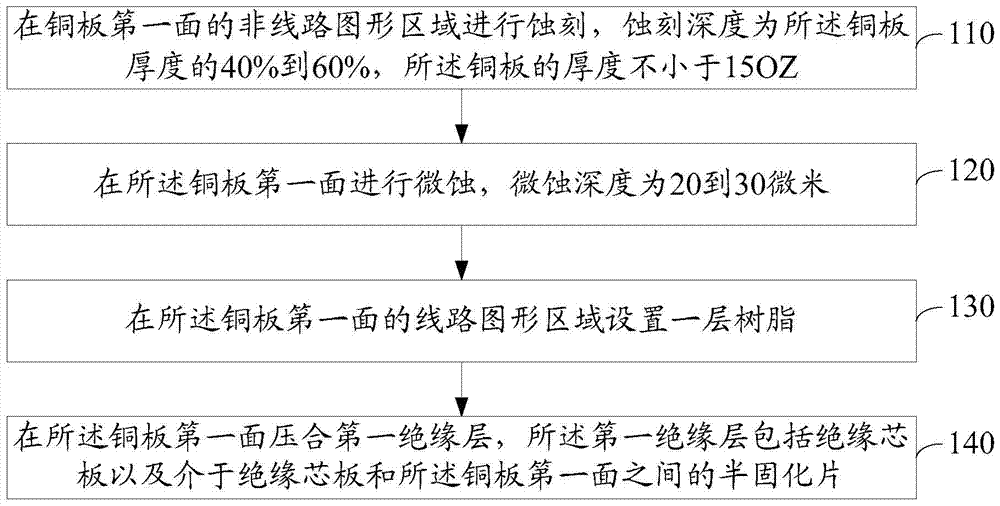
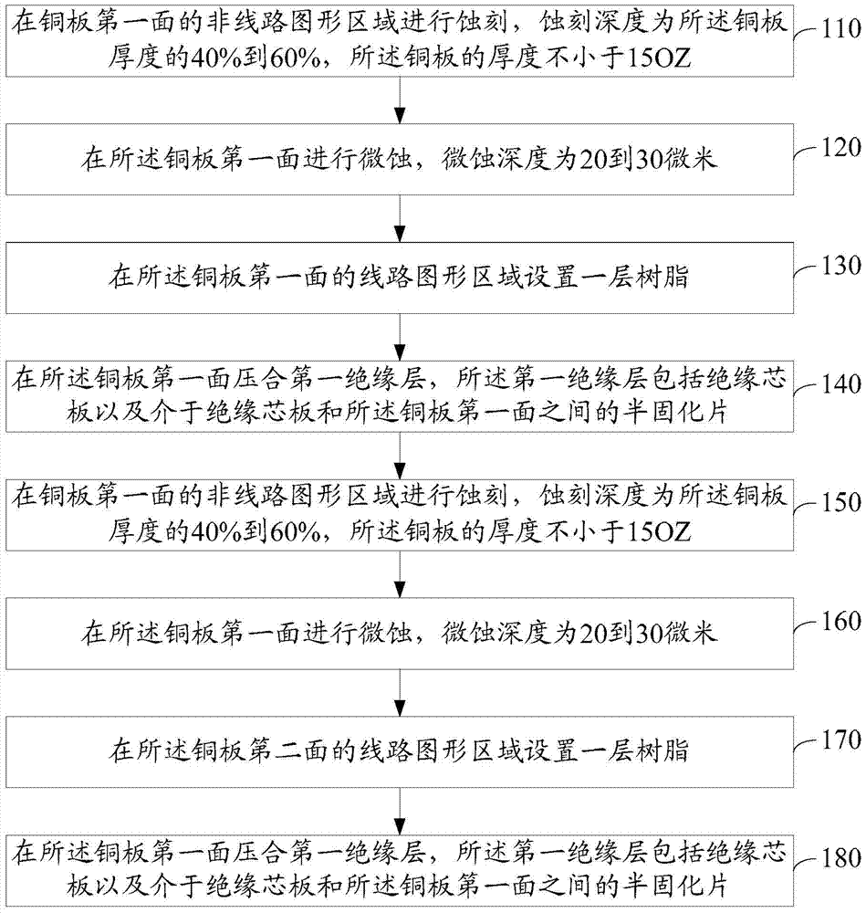
[0019] Please refer to figure 1 , the embodiment of the present invention provides a thick copper circuit board processing method, comprising:

[0020] 110. Etching the non-circuit pattern area on the first surface of the copper plate, the etching depth is 40% to 60% of the thickness of the copper plate, and the thickness of the copper plate is not less than 15OZ.

[0021] In the embodiment of the present invention, a double-sided etching process is used to process circuit patterns on a copper plate with a thickness not less than 15 OZ. First, the first etching is carried out, including: covering the circuit pattern area on the first surface of the copper plate with a resist film, etching the non-circuit pattern area into a groove whose depth is about half the thickness of the copper plate, and then removing the resist film. As for the unetched part of the bottom of the groove, it is left to be removed by the next etching. After the first etching is completed, the circuit pa...


PUM

PropertyMeasurementUnit
thicknessaaaaaaaaaa

Abstract

The invention discloses a processing method of a thick copper circuit board. The processing method comprises the steps of etching a non-line graph area of the first surface of a copper plate, wherein the etching depth is 40% to 60% of the thickness of the copper plate, and the thickness of the copper plate is not less than 15 OZ; microetching the first surface of the copper plate, wherein the microetching depth is 20 to 30 micrometers; applying a layer of resin in a line graph area of the first surface of the copper plate; pressing a first insulating layer on the first surface of the copper plate, wherein the first insulating layer comprises an insulating core plate and a prepreg which is arranged between the insulating core plate and the first surface of the copper plate. According to the technical scheme of the processing method, burrs on a shoulder of a line after etching can be eliminated, so that the problem of cracks caused by mechanical squeezing of the burrs on glass fiber is avoided; a large quantity of bubbles remained in the resin can be avoided, so as to avoid layering or delamination caused the bubbles during subsequent pressing; the subsequent drilling difficulty can be reduced, and the breaking risk is reduced; the thickness uniformity of the obtained thick copper circuit board can be increased.

Description

technical field [0001] The invention relates to the technical field of circuit boards, in particular to a method for processing thick copper circuit boards. Background technique [0002] With the increasing demand for high current of power supply products, the copper layer of the circuit board is getting thicker and thicker, the lines are getting denser, the current is getting bigger and bigger, and the withstand voltage requirements are getting higher and higher. When the copper thickness exceeds 1mm, there will be more difficulties and problems in the conventional PCB process, especially in the lamination process. [0003] In the prior art, for thick copper products, conventional prepreg (PP) lamination is generally used, or resin is firstly filled and then PP lamination is performed. This lamination process has the following defects: [0004] 1. The conventional PP lamination process refers to the direct use of PP to laminate the outer layer on the etched side of the th...

Claims


Application Information

Patent Timeline
Patent Type & Authority Patents(China)
IPC IPC(8): H05K3/00H05K3/06
CPCH05K3/06H05K3/28H05K2201/0959H05K2203/1476
Inventor 黄立球刘宝林
Owner SHENNAN CIRCUITS
Why Eureka
Try Eureka