Preparation method and substrate of transparent single crystal Aln, ultraviolet light-emitting device

A technology for light-emitting devices and single crystals, which is used in semiconductor devices, semiconductor/solid-state device manufacturing, and electrical components. The effect of avoiding oxidation problems

Active Publication Date: 2021-06-18
INST OF SEMICONDUCTORS - CHINESE ACAD OF SCI
View PDF0 Cites 0 Cited by
  • Summary
  • Abstract
  • Description
  • Claims
  • Application Information

AI Technical Summary

Problems solved by technology

However, the shortcomings of the MOCVD process are: it is difficult to overcome the stress and high dislocation problems caused by heterogeneous epitaxy; and the material growth rate of the MOCVD process is slow (hundreds of nanometers per hour), which is not suitable for preparing commercial AlN monolayers with a thickness of several hundred microns. crystal substrate material; in addition, metal aluminum organic compound TMAl and NH 3 severe pre-reaction
However, the disadvantages of the HVPE process are: it is difficult to directly grow heterogeneous epitaxy to obtain a material with a flat surface and high crystallinity; A complete and large-area unsupported AlN thick-film single crystal material is obtained by peeling off the bottom. The yield of the material is low and it is not suitable for commercialization.
However, the disadvantages of the PVT process are: the growth temperature of the material is very high, and there are high requirements for the temperature gradient control of the growth chamber; the AlN single crystal obtained by PVT growth is mostly orange and brown, and the light transmission is not good; control
[0011] 1. The problem of ultraviolet light absorption by the AlN single crystal substrate prepared by PVT is still unsolved. Therefore, after obtaining the HVPE-AlN single crystal, in order to improve the luminous performance of the deep ultraviolet light-emitting device, it is necessary to use chemical mechanical polishing (CMP ) method to remove the PVT-AlN substrate with poor light transmittance, and this PVT-AlN substrate is a high-quality single crystal AlN material, which is extremely expensive. Therefore, grinding away this substrate material to obtain an AlN single crystal results in A great waste is caused, and thus the production cost of the deep ultraviolet light-emitting device is increased;
[0012] 2. The CMP process itself is time-consuming and labor-intensive, and the surface of the processed material is uneven, which is prone to oxidation problems;
[0013] 3. The AlN grown by the HVPE process will have a lot of stress, and it is prone to cracks and other problems during the grinding and polishing process.

Method used


Image

  • Preparation method and substrate of transparent single crystal Aln, ultraviolet light-emitting device
  • Preparation method and substrate of transparent single crystal Aln, ultraviolet light-emitting device
  • Preparation method and substrate of transparent single crystal Aln, ultraviolet light-emitting device

Examples


Embodiment Construction

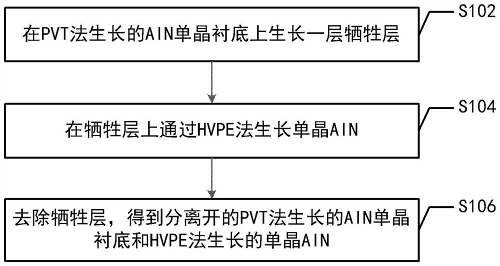
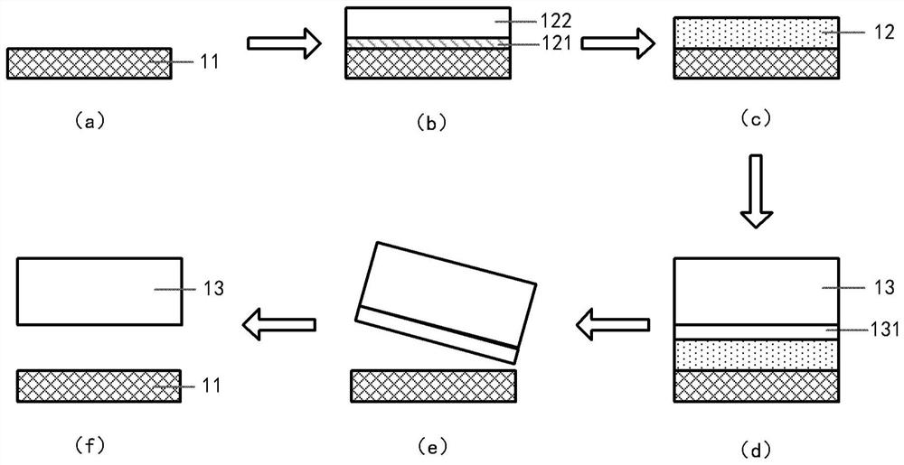
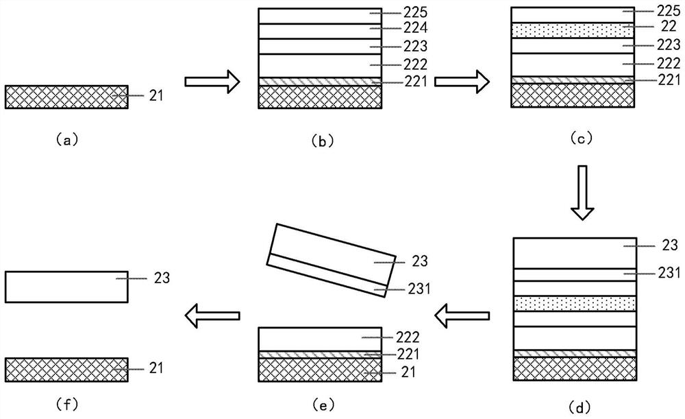
[0047] The disclosure provides a method for preparing transparent single crystal AlN, a substrate, and an ultraviolet light-emitting device. A sacrificial layer is grown on the AlN single crystal substrate grown by the PVT method, and then a single crystal is grown on the sacrificial layer by the HVPE method. AlN, and remove the sacrificial layer to obtain separated AlN single crystal substrate grown by PVT method and single crystal AlN grown by HVPE method, no need for chemical mechanical polishing, only need to simply remove the thinner sacrificial layer, fast and effective, At the same time, the oxidation problem caused by CMP is avoided, and the AlN single crystal substrate grown by the PVT method is preserved, and can be returned to the furnace to continue making seed crystals for epitaxy to realize recycling; the oxygen and carbon of the obtained single crystal AlN grown by the HVPE method The content of impurities is very low, and it is transparent single crystal AlN, wh...


PUM


Abstract

The invention discloses a method for preparing a transparent single crystal AlN, a substrate, and an ultraviolet light-emitting device, wherein the method for preparing a transparent single crystal AlN comprises: growing a sacrificial layer on an AlN single crystal substrate grown by a PVT method, the The sacrificial layer is: a conductive porous structure, a porous structure self-decomposed by thermal stress, or a polycrystalline buffer layer grown at low temperature; a single crystal AlN is grown on the sacrificial layer by HVPE; and the sacrificial layer is removed by electrochemical etching or laser lift-off , or directly use thermal stress to realize self-separation of the sacrificial layer, and obtain separated AlN single crystal substrate grown by PVT method and single crystal AlN grown by HVPE method. Only the thinner sacrificial layer needs to be simply removed, which is fast and effective, and at the same time avoids the oxidation problem caused by CMP, and the AlN single crystal substrate grown by the PVT method can be retained to realize recycling and effectively reduce the cost of transparent single crystal AlN substrate. The production cost of the bottom material. However, the single crystal AlN grown by HVPE method has high transmittance in the ultraviolet band, which is more suitable for the preparation of ultraviolet light-emitting devices.

Description

technical field [0001] The disclosure belongs to the technical field of semiconductor material preparation, and relates to a preparation method of transparent single crystal AlN, a substrate, and an ultraviolet light-emitting device. Background technique [0002] The third-generation semiconductor materials are wide-bandgap semiconductor materials represented by gallium nitride (GaN), silicon carbide (SiC), aluminum nitride (AlN), etc., due to their wide bandgap width and high breakdown electric field , high thermal conductivity, high thermal stability, corrosion resistance and radiation resistance and other excellent physical and chemical properties, widely used in high frequency, microwave power devices, light emitting devices and other fields. Compared with GaN and SiC, AlN material has a wider forbidden band width, so it can be used as a substrate material for the preparation of deep ultraviolet light-emitting diodes (LEDs), ultraviolet laser diodes (LDs) and sun-blind d...

Claims


Application Information

Patent Timeline
Patent Type & Authority Patents(China)
IPC IPC(8): H01L21/02H01L33/00
CPCH01L21/02389H01L21/02436H01L21/02458H01L21/0254H01L21/0262H01L21/02631H01L33/00
Inventor 刘乃鑫魏同波魏学成王军喜李晋闽
Owner INST OF SEMICONDUCTORS - CHINESE ACAD OF SCI
Why Eureka
Try Eureka