A method of manufacturing a pcb with bottomless copper metallized blind holes

A technology for metallized blind holes and manufacturing methods, which is applied in the fields of printed circuit manufacturing, electrical connection formation of printed components, electrical components, etc., can solve copper edge roughness, make non-metallized blind holes into bottomless copper metallized blind holes, Affect the quality of bottomless copper metallized blind holes, etc., to avoid large area and improve quality

Inactive Publication Date: 2017-10-17
SHENZHEN SUNTAK MULTILAYER PCB
View PDF6 Cites 0 Cited by
  • Summary
  • Abstract
  • Description
  • Claims
  • Application Information

AI Technical Summary

Problems solved by technology

However, according to the existing technology, it is difficult to directly make non-metallized blind holes into bottomless copper metallized blind holes. The existing method is to first make non-metallized blind holes into metallized blind holes, and then make the outer layer Circuit, after making the outer layer circuit, mill the copper at the bottom of the metalized blind hole by milling the bottom copper, so as to form a bottomless copper metalized blind hole on the PCB
In the existing manufacturing method, in order to prevent the copper plating on the hole wall from being damaged, it is necessary to pre-mill the length and width of the bottom copper. Therefore, after the bottom copper is milled off, a large area of ​​copper will remain near the bottom of the hole and the hole wall, and the cut The copper edge will be very rough, seriously affecting the quality of bottomless copper metallized blind holes

Method used


Image

  • A method of manufacturing a pcb with bottomless copper metallized blind holes
  • A method of manufacturing a pcb with bottomless copper metallized blind holes
  • A method of manufacturing a pcb with bottomless copper metallized blind holes

Examples


Embodiment 1

[0018] This embodiment provides a method for manufacturing a PCB with bottomless copper metallized blind holes. The specific manufacturing steps are as follows:

[0019] (1) Pressing to form a multi-layer board

[0020] Firstly, as in the PCB production process of the prior art, the raw materials of the PCB are cut to obtain a core board, and then the inner layer circuit is produced on the core board by using a negative film process. Through the AOI inspection of the inner layer, check whether there are defects such as open and short circuits, line gaps, and line pinholes in the inner layer lines, and products without defects enter the lamination process.

[0021] Carry out browning treatment on the core board, then stack the core board, prepreg and outer copper foil according to the design data, and then select appropriate pressing conditions according to the Tg of the board material, and press the stacked boards into one to form a multilayer board.

[0022] (2) Making meta...

Embodiment 2

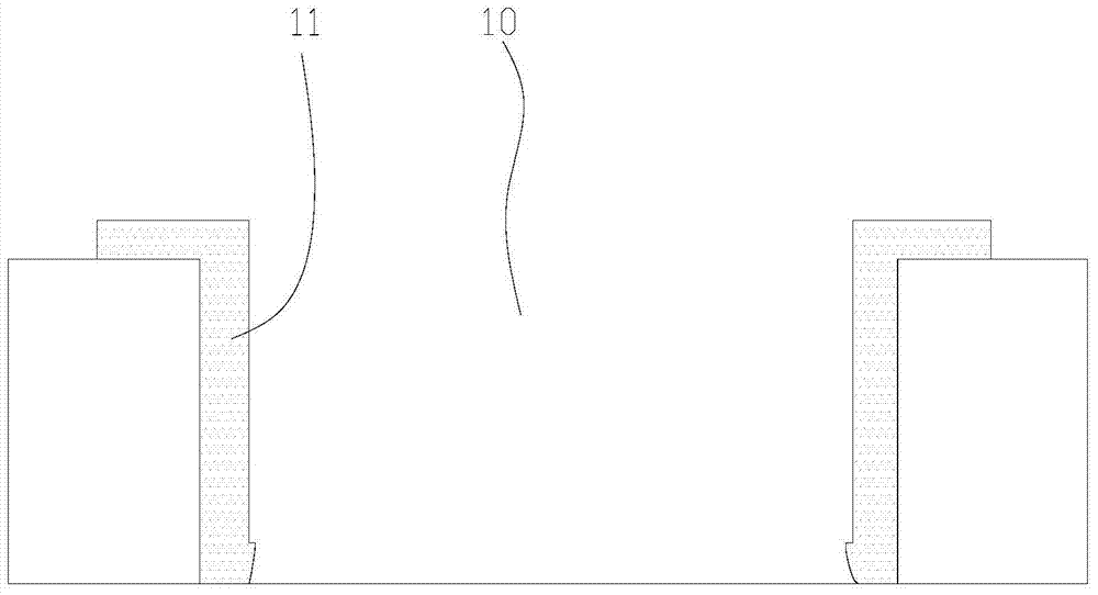
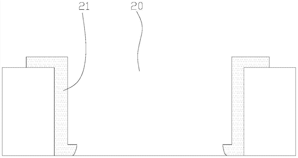
[0033] This embodiment provides a method for manufacturing a PCB with bottomless copper metallized blind holes. The specific manufacturing steps are basically the same as those in Embodiment 1, the difference being that: the metallized blind holes are cut through controlled depth milling. When the copper layer at the bottom of the hole is removed, the vertical distance between the milling edge and the wall of the metallized blind hole is 0.03mm, that is, when the copper at the bottom of the hole is milled, the milling edge shrinks 0.03mm inward compared to the single side of the hole wall.

[0034] The schematic diagram of the cross-sectional structure of the bottomless copper metallized blind hole 20 produced is as follows figure 2 shown. The milled edge becomes smooth after the outer layer is etched, but the milled edge obviously protrudes from the hole wall 21 , so that the residual copper edge area at the bottom of the bottomless copper metallized blind hole 20 is relativ...

Embodiment 3

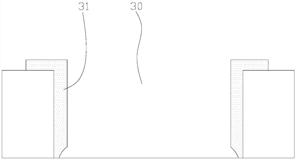
[0036] This embodiment provides a method for manufacturing a PCB with bottomless copper metallized blind holes. The specific manufacturing steps are basically the same as those in Embodiment 1, the difference being that: the metallized blind holes are cut through controlled depth milling. When the copper layer at the bottom of the hole is removed, the vertical distance between the milling edge and the hole wall of the metallized blind hole is 0.005mm, that is, when the copper at the bottom of the hole is milled, the milling edge shrinks 0.005mm from the single side of the hole wall.

[0037] The schematic diagram of the section structure of the bottomless copper metallized blind hole 30 produced is as follows image 3 shown. The milling edge becomes smooth after the outer layer is etched, but the milling edge is obviously recessed into the hole wall 31 .

[0038] In other embodiments, when the copper layer at the bottom of the metallized blind hole is removed by controlled de...


PUM


Abstract

The invention relates to the technical field of PCB manufacturing, in particular to a manufacturing method of a PCB with a base copper-free metallized blind hole. The manufacturing method comprises the following steps: firstly manufacturing a metallized blind hole, then performing pattern plating, adopting a depth controlled milling manner to remove a copper layer at the bottom of the hole before outer layer etching, and then etching the copper edge remaining at the bottom of the metallized blind hole through the outer layer etching, so that the milled edge is smooth, the problems that the copper edge remaining at the bottom of the base copper-free metallized blind hole is large in area and coarse can be avoided, and the quality of the base copper-free metallized blind hole is greatly improved; setting the perpendicular distance between the milled edge and the wall of the metallized blind hole to be 0.01-0.02 mm, and enabling the milled edge after outer layer etching to be basically flush with the hole wall; setting the depth controlled milling to be 0.1-0.11 mm deeper than the metallized blind hole, so as to ensure that the copper layer at the bottom of the hole is completely removed, and no influence is generated due to nonuniformity of the copper layer.

Description

technical field [0001] The invention relates to the technical field of PCB manufacturing, in particular to a method for manufacturing a PCB provided with bottomless copper metallized blind holes. Background technique [0002] PCB (Printed Circuit Board) is one of the important components of the electronics industry, a support for electronic components, and a carrier for electrical connections. With the increase in functions and the reduction in volume of electronic products, PCBs are constantly developing in the direction of diversification, high density, and miniaturization. Bottomless copper metallized blind holes are designed on the PCB (that is, the wall of the blind hole has copper and the bottom of the hole has no copper), which is used to install and fix the device on it to achieve certain specific functions. This is the diversification of PCB. reflect. However, according to the existing technology, it is difficult to directly make non-metallized blind holes into bo...

Claims


Application Information

Patent Timeline
Patent Type & Authority Patents(China)
IPC IPC(8): H05K3/42
CPCH05K3/421H05K2201/09509H05K2203/0228
Inventor 翟青霞彭君赵波周文涛王佐
Owner SHENZHEN SUNTAK MULTILAYER PCB
Why Eureka
Try Eureka