Double FP-cavity optical fiber acoustic sensing probe and sensing system thereof
A sensing probe and sensing system technology, applied in the direction of sensors, sensor parts, electrical components, etc., can solve the problems of not reducing the difficulty of the optical fiber FP cavity sensitive head, the process has no advantages, the signals are no longer orthogonal, etc., and the cost is achieved Low, simple structure, high sensitivity effect
- Summary
- Abstract
- Description
- Claims
- Application Information
AI Technical Summary
Problems solved by technology
Method used
Image
Examples
Embodiment 1
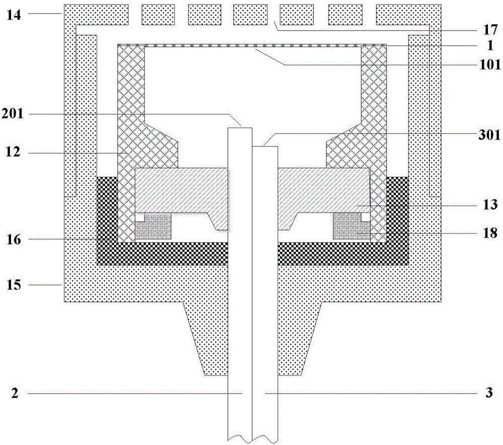
[0058] like figure 1 Shown is a double FP-cavity optical fiber acoustic sensor probe structure implemented according to the present invention, including: a diaphragm 1 sensitive to acoustic signals, light guide units 2 and 3 as optical fibers, an upper structure 12 and a lower structure 13 . The diaphragm 1 is mounted on the front end of the upper structure 12 . The light guide units 2 and 3 are installed in the lower structure body 13 , and the lower ends of the light guide units 2 and 3 are light input ends. The lower structure body 13 is placed in the accommodation space of the upper structure body 12, and the upper end surface 201 of the light guide unit 2 installed in the lower structure body 13 and the upper end surface 301 of the light guide unit 3 respectively form an FP cavity with the reflective surface 101 of the diaphragm 1 , the height difference between the end face 201 and the end face 301 is an odd multiple of one-eighth of the working light wavelength; a lock...
Embodiment 2
[0060] like Figure 4 Shown is a dual-FP-cavity optical fiber acoustic sensor probe structure using MEMS technology according to an embodiment of the present invention, including: a diaphragm 1 sensitive to acoustic signals, light-transmitting optical fibers 202 and 302, a silicon wafer structure 19, and a glass structure Body 20. The diaphragm 1 is located at the front end of the silicon wafer structure 19, and is made of silicon material or deposited silicon nitride material; the upper surface of the glass structure 20 is etched along the symmetrical center line to form two planes 201 and 301 with different heights, and the planes 201 and 301 The height difference is an odd multiple of one-eighth of the wavelength of the working light. A pit is made in the center of the lower surface of the glass structure 20, and the light-transmitting optical fibers 202 and 302 are placed in the pit and fixed with glue with a similar refractive index; wherein the light-transmitting optica...
PUM
 Abstract
Description
Claims
Application Information


