
Clamp for thermal resistance test of SMD packaged semiconductor device

A test fixture and semiconductor technology, which is applied in the direction of single semiconductor device testing, measuring device casing, etc., can solve the problems of electrode short circuit and inability to test, and achieve the effects of fast measurement, good electrical contact and heat transfer, and low cost

Inactive Publication Date: 2015-06-24
THE 13TH RES INST OF CHINA ELECTRONICS TECH GRP CORP
View PDF9 Cites 15 Cited by
  • Summary
  • Abstract
  • Description
  • Claims
  • Application Information

AI Technical Summary

Problems solved by technology

[0004] For semiconductor devices packaged in SMD (Surface Mount Devices, Surface Mount Devices), the three electrodes are all located on the bottom of the device and on the same plane. Since the part with a higher temperature of the casing is the bottom surface of the lead-out electrode during operation, the control casing When the temperature is high, it is necessary to stick the electrode surface to the temperature control platform and the thermocouple probe, but the temperature control platform is made of metal. If the device is directly attached to the temperature control platform, it will inevitably fail to test due to the short circuit of the electrodes.

Method used


Image

  • Clamp for thermal resistance test of SMD packaged semiconductor device
  • Clamp for thermal resistance test of SMD packaged semiconductor device

Examples


Embodiment Construction

[0021] The present invention will be further described in detail below in conjunction with the accompanying drawings and specific embodiments.

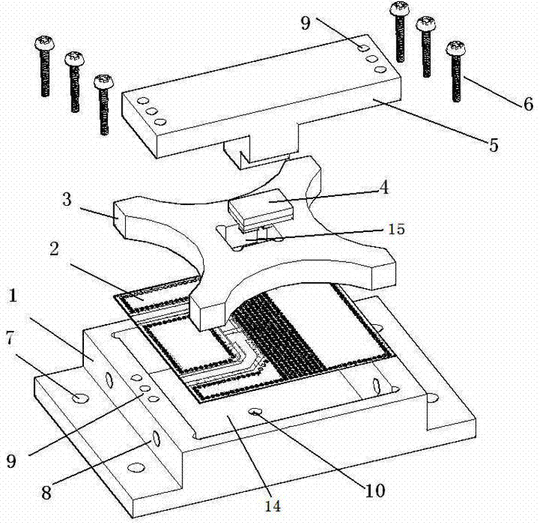
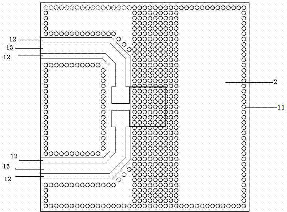
[0022] Such as figure 1 As shown, a jig for testing thermal resistance of an SMD packaged semiconductor device includes a metal base 1 , a PCB circuit board 2 , an insulating positioning block 3 and a pressing block 5 . The metal base 1 is made of copper, and the metal base 1 is provided with a groove 14, and the thickness of the bottom of the groove 14 is 1 mm. The PCB circuit board 2 is placed in the groove 14, and the conductive silver paste or conductive paper is coated between the PCB circuit board 2 and the groove 14. The PCB circuit board 2 is a nickel-plated gold circuit board, and the thickness of the PCB circuit board 2 is 0.5mm, the nickel-plated gold circuit board has good thermal conductivity, which is beneficial to the heat transfer between the tested SMD device 4 and the constant temperature platform. The PCB circuit ...


PUM

PropertyMeasurementUnit
Thicknessaaaaaaaaaa
Diameteraaaaaaaaaa
Thicknessaaaaaaaaaa

Abstract

The invention discloses a clamp for a thermal resistance test of a SMD packaged semiconductor device and relates to the technical field of semiconductor testing. The clamp comprises a metal base, a PCB, an insulated locating block and a compressing block. A groove is formed in the metal base. The PCB circuit is arranged in the groove. The insulated locating block is arranged on the PCB. The insulated locking block is provided with a locating containing hole matched with the tested SMD device. The compressing block capable of downwards compressing a tested SMD device is arranged on the insulated locating block. A thermocouple probe containing hole corresponding to the electrode of the tested SMD device in position is formed in the bottom of the groove. Two electrode wiring holes are formed in the side faces of the groove. Two electrodes enabling pins of the tested SMD device to be connected with electrode wiring holes are arranged on the PCB. The clamp can guarantee that the good thermal conductivity between the tested SMD device and a constant-temperature platform is achieved, the temperature of a shell can be easily controlled within a required range, it is also guaranteed that the electrodes of the tested SMD device are insulated from one another, and normal operation of the test is guaranteed.

Description

technical field [0001] The invention relates to the technical field of semiconductor testing. Background technique [0002] The thermal characteristics of semiconductor devices are one of the important contents in reliability design. In order to ensure the reliability of the device in use, the structural design of the device should consider the heat dissipation characteristics of the device, and the quantitative calculation of these designs needs to be based on the thermal resistance parameters of the device. Therefore, the thermal resistance of a semiconductor device is an important parameter reflecting the thermal characteristics of the device. [0003] The resistance encountered by heat on the heat conduction path is thermal resistance. It is defined as the ratio of the temperature difference on the heat conduction path to the power consumption. The thermal resistance of the device junction to the case is the thermal resistance between the heat source junction of the c...

Claims


Application Information

Patent Timeline
IPC IPC(8): G01R1/04G01R31/26
Inventor 茹志芹迟雷彭浩张瑞霞林奇全
Owner THE 13TH RES INST OF CHINA ELECTRONICS TECH GRP CORP
Learn More