
Display and its gate drive circuit and gate drive unit circuit

A unit circuit and gate drive technology, applied in static indicators, instruments, etc., can solve the problems of short life of GOA, achieve long working life, and suppress the drift speed of threshold voltage

Active Publication Date: 2017-05-10
PEKING UNIV SHENZHEN GRADUATE SCHOOL
View PDF4 Cites 0 Cited by
  • Summary
  • Abstract
  • Description
  • Claims
  • Application Information

AI Technical Summary

Problems solved by technology

However, the threshold voltage drift of the pull-down transistor is still unavoidable, so the lifetime of GOA is still short

Method used


Image

  • Display and its gate drive circuit and gate drive unit circuit
  • Display and its gate drive circuit and gate drive unit circuit
  • Display and its gate drive circuit and gate drive unit circuit

Examples


Embodiment 1

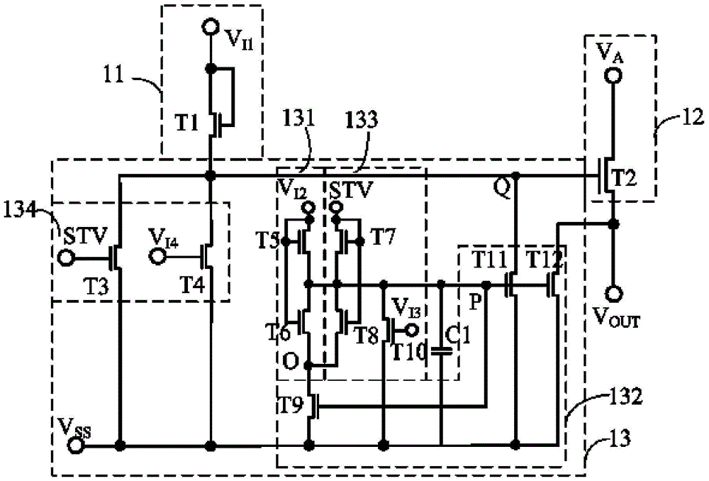
[0044] Please refer to figure 1 , this embodiment provides a gate driving unit circuit, including an input module 11 , a driving module 12 and a low level maintaining module 13 .

[0045] The input module 11 is coupled between the first pulse signal terminal and the first node Q, for responding to the first pulse signal V I1 The high level of the first node Q is charged.

[0046] The control terminal of the driving module 12 is used to be coupled to the first node Q, and its input terminal is used to input the first clock signal V A , whose output is used to couple to the signal output V OUT , the drive module 12 sends the first clock signal V to the first node Q in response to the high-level signal A Applied to the signal output terminal V OUT .

[0047] The low level maintaining module 13 includes a first charging unit 131 and a threshold voltage self-compensating unit 132 .

[0048] The first charging unit 131 includes a fifth transistor T5 and a sixth transistor T6, ...

Embodiment 2

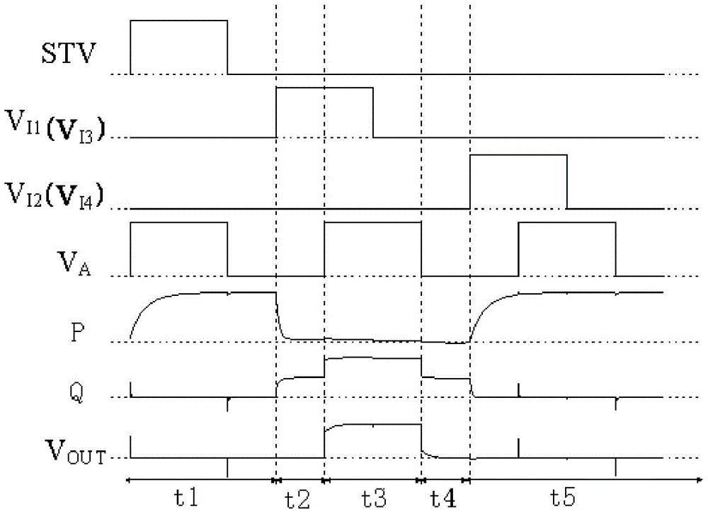
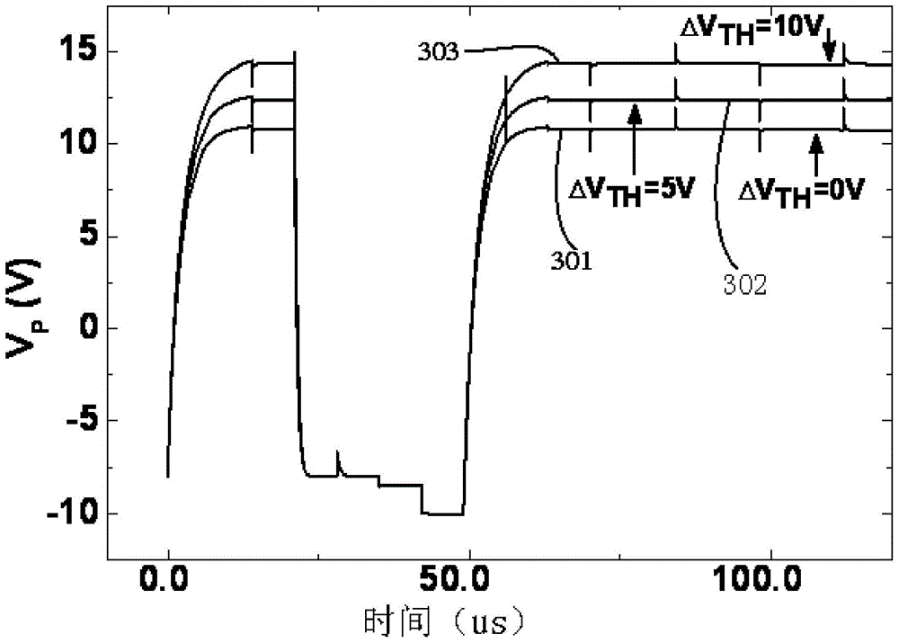
[0068] In the gate drive unit circuit provided in Embodiment 1, the gate drive unit circuit works in the low-level maintenance stage most of the time , In the low-level maintenance phase, the fifth transistor T5, the sixth transistor T6, the seventh transistor T7, the eighth transistor T8, the ninth transistor T9, and the tenth transistor T10 are in the off state, and the voltage on the second node P needs to ensure that the first The eleventh transistor T11 and the twelfth transistor T12 are in the on state to connect the first node Q and the signal output terminal V OUT pulled down to the first low level V SS ; Because the fifth transistor T5, the sixth transistor T6, the seventh transistor T7, the eighth transistor T8, the ninth transistor T9, and the tenth transistor T10 have leakage currents passing through, the voltage of the second node P will drop slowly, thereby causing the tenth The conduction capability of the first transistor T11 and the twelfth transistor T12 dec...

Embodiment 3

[0081] Please refer to Figure 7 , based on the gate drive unit circuit provided in Embodiment 1, this embodiment accordingly provides a gate drive circuit, including N cascaded gate drive unit circuits, where N is a positive integer greater than or equal to 4, and the gate The driving unit circuit is the gate driving unit circuit provided in the first embodiment.

[0082] The gate drive circuit also includes a first clock line CK1, a second clock line CK2, a third clock line CK3, a fourth clock line CK4, a first pulse signal line V 1 , the second pulse signal line V 2 , the third pulse signal line V 3 , the fourth pulse signal line V 4 , the initial set signal line ST and the first low-level signal line V S ; The high level arrival time of the clock signal output by the second clock line CK2 lags behind the high level arrival time T / 4 of the clock signal output by the first clock line CK1, and the high level of the clock signal output by the third clock line CK3 The arri...


PUM


Abstract

The invention provides a display device and a gate drive circuit and a gate drive unit circuit thereof, the gate drive unit circuit comprises an input module, a driving module and a low level maintaining module, and the low level maintaining module comprises a first charging unit and a threshold voltage self compensating unit. The voltage of a second node P in the threshold voltage self compensating unit changes along with the threshold voltage of a drop-down transistor in the low level maintaining module in a self-adaptive mode, therefore, the gate overdrive voltage of the drop-down transistor maintains a constant value, the drift amplitude of the threshold voltage of the drop-down transistor is increased, due to the fact that the overdrive voltage value is small, and the drift speed of the threshold voltage of the drop-down transistor is restrained, the gate drive unit circuit has the advantage of being long in working life.

Description

technical field [0001] The present application relates to a display and its gate drive circuit and gate drive unit circuit, in particular to a gate drive circuit suitable for large-size and high-resolution TV panels. Background technique [0002] Thin-film transistor (TFT) flat panel display (Flat Panel Display, FPD) technology is the mainstream of display technology today, and large-size, high-resolution display is an important development direction of TFT-FPD. TFT integrated gate driver circuit (GateDriver OnArray, GOA) is an important technology in the development of large-size, high-resolution TFT-FPD. Compared with the traditional method, that is, the use of peripheral gate drive ICs, the number of external leads of GOA's TFT-FPD panel is greatly reduced, so the limitation of the resolution caused by too dense leads is relaxed. Other advantages brought by GOA technology include: reducing the number of peripheral ICs used, making signal transmission more stable and reli...

Claims


Application Information

Patent Timeline
Patent Type & Authority Patents(China)
IPC IPC(8): G09G3/20
Inventor 张盛东李文杰廖聪维胡治晋李君梅
Owner PEKING UNIV SHENZHEN GRADUATE SCHOOL
Learn More