Soft landing nanolaminates for advanced patterning

A nano-lamination and patterning technology, applied in nanotechnology, coating, gaseous chemical plating, etc.

Inactive Publication Date: 2015-07-01
NOVELLUS SYSTEMS
View PDF5 Cites 22 Cited by
  • Summary
  • Abstract
  • Description
  • Claims
  • Application Information

AI Technical Summary

Problems solved by technology

There are challenges in the magnitude expansion of multi-patterning technology to 11nm half-pitch and below

Method used


Image

  • Soft landing nanolaminates for advanced patterning
  • Soft landing nanolaminates for advanced patterning
  • Soft landing nanolaminates for advanced patterning

Examples


Embodiment Construction

[0027] In the following description, numerous specific details are set forth in order to provide a thorough understanding of the presented embodiments. The disclosed embodiments may be practiced without some or all of these specific details. In other instances, well known method operations have not been described in detail in order not to unnecessarily obscure the disclosed embodiments. While the disclosed embodiments will be described in conjunction with specific embodiments, it will be understood that these embodiments are not intended to limit the disclosed embodiments.

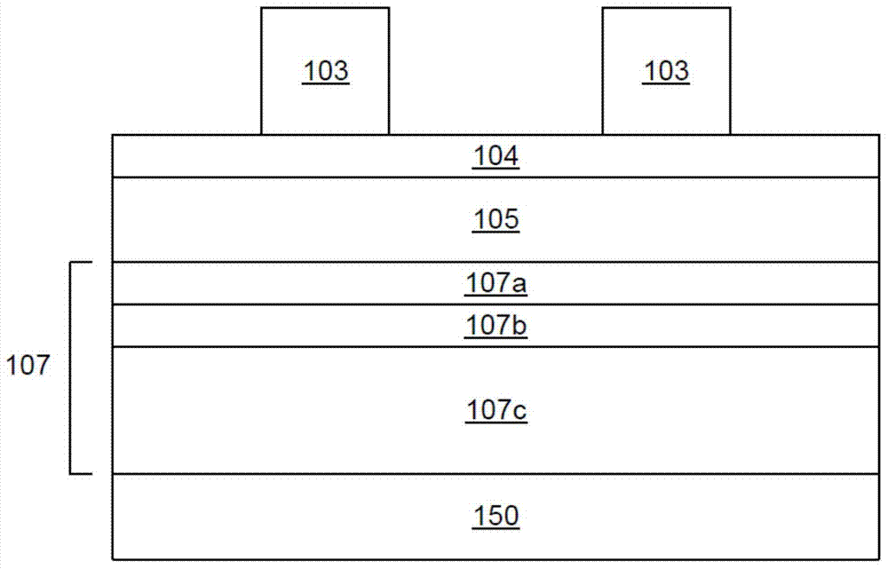
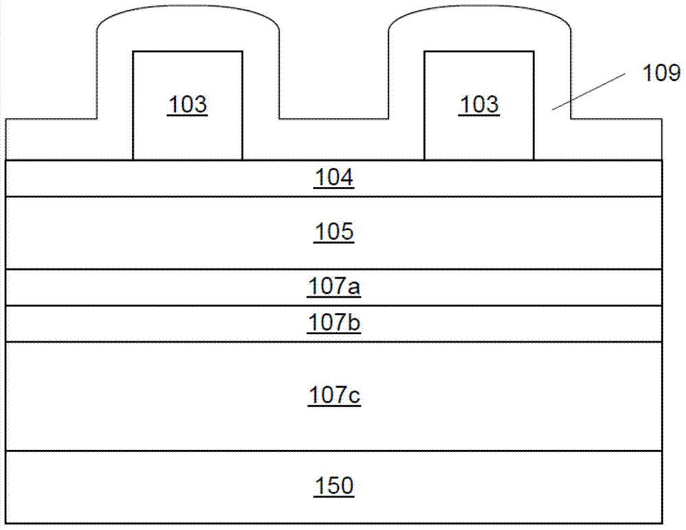
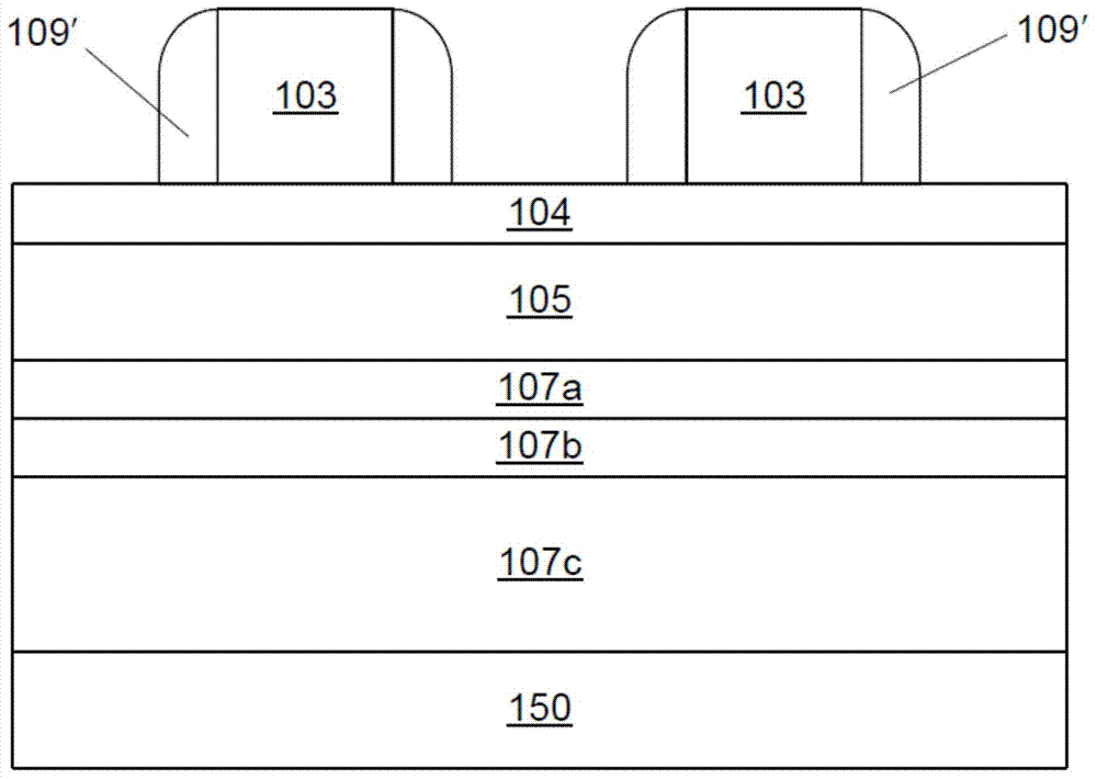
[0028] Fabricating a semiconductor device typically involves depositing one or more thin films in an integrated fabrication process and may include a patterning step. Multi-patterning techniques are used to fabricate advanced integrated circuits, for example, with smaller features or higher aspect ratios or down to 2x or 1x nm nodes. The term "1x" node means a processing node between 10nm and 19nm, and t...


PUM


Abstract

Methods for depositing nanolaminate protective layers over a core layer to enable deposition of high quality conformal films over the core layer for use in advanced multiple patterning schemes are provided. In certain embodiments, the methods involve depositing a thin silicon oxide or titanium oxide film using plasma-based atomic layer deposition techniques with a low high frequency radio frequency (HFRF) plasma power, followed by depositing a conformal titanium oxide film or spacer with a high HFRF plasma power.

Description

technical field [0001] The present invention relates to methods of processing substrates, and more particularly to methods for depositing a nanolaminate protective layer on a core layer to allow deposition of high quality conformal films on the core layer for use in advanced multi-patterning schemes. Background technique [0002] Advanced integrated circuits typically involve patterning 1x nm half-pitch features in high-volume semiconductor fabrication. Multiple patterning techniques may allow scaling of feature sizes according to lithographic techniques such as immersion lithography at 193nm. Self-aligned double patterning is an example of a multi-patterning technique. There are challenges in the magnitude expansion of multi-patterning technology to 11nm half-pitch and below. Contents of the invention [0003] Provided herein are methods for processing semiconductor substrates to allow deposition of high quality conformal films for use in multi-patterning integration sc...

Claims


Application Information

Patent Timeline
Patent Type & Authority Applications(China)
IPC IPC(8): H01L21/316H01L21/311B82Y40/00
CPCC23C16/45542H01L21/02164H01L22/12H01L21/02274H01L21/02219H01L22/20C23C16/345C23C16/401C23C16/4554H01L21/0217C23C16/405H01L21/02186H01L21/0228H01L21/0337H01L21/0332C23C16/402C23C16/505C23C16/56H01L21/0273H01L21/31144
Inventor 弗兰克·L·帕斯夸里尚卡·斯瓦米纳森阿德里安·拉瓦伊纳德·沙姆玛吉里什·迪克西特
Owner NOVELLUS SYSTEMS
Why Eureka
Try Eureka