Fin type field-effect transistor and forming method thereof

A fin field effect and transistor technology, which is applied in semiconductor devices, semiconductor/solid state device manufacturing, electrical components, etc., can solve problems such as uneven distribution of impurity ions and affect the performance of fin field effect transistors, and achieve the effect of improving performance

Active Publication Date: 2015-07-01
SEMICON MFG INT (SHANGHAI) CORP
View PDF3 Cites 9 Cited by
  • Summary
  • Abstract
  • Description
  • Claims
  • Application Information

AI Technical Summary

Problems solved by technology

[0005] In the prior art, the source / drain region 17 formed in the fin portion 14 on both sides of the gate structure 12 is prone to defects of uneven distribution of impurity ions, which affects the performance of the FinFET

Method used


Image

  • Fin type field-effect transistor and forming method thereof
  • Fin type field-effect transistor and forming method thereof
  • Fin type field-effect transistor and forming method thereof

Examples


Embodiment Construction

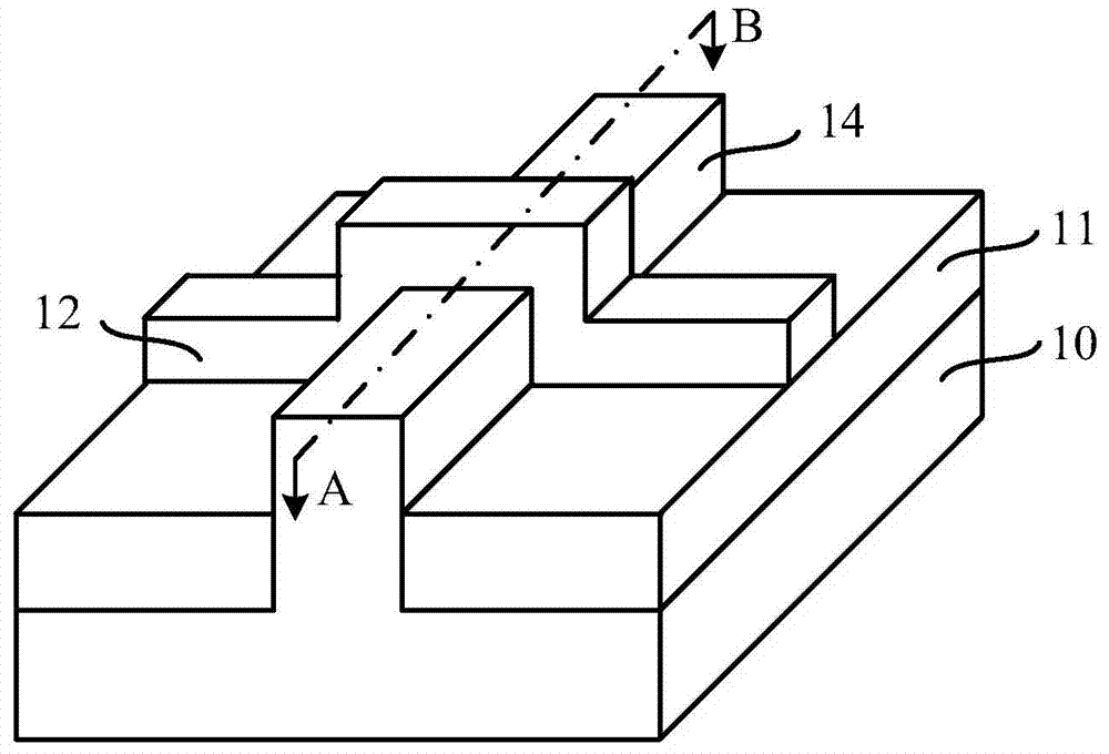
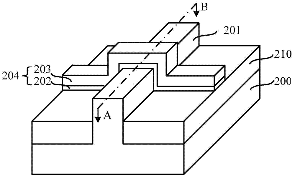
[0034] After research, since the fin is a three-dimensional structure, including a top surface and two side surfaces, when the source / drain region is formed in the fin on both sides of the gate structure by ion implantation, it is very easy to make the formation of the source / drain region The distribution of impurity ions is uneven, for example, the impurity ion concentration at the bottom of the fin (the bottom of the source / drain region) is small, and the top surface and sidewall surfaces of the fins near the gate structure (the top and both sides of the source / drain region There is a large difference in the distribution concentration of impurity ions on the side wall. Since the fin field effect transistor works, the channel is formed on the top surface and the sidewall surfaces on both sides of the fin at the bottom of the gate structure. If the impurity ions are unevenly distributed, the amount of current passing through the channel on the top surface of the fin and the ch...


PUM


Abstract

Provided are a fin type field-effect transistor and a forming method thereof. The forming method of the fin type field-effect transistor comprises the steps of providing a semiconductor substrate, forming a fin portion on the semiconductor substrate, forming gate electrode structures on the surfaces of the top and the side wall of the fin portion and forming side walls on two side walls of each gate electrode structure; etching the fin portions on two sides of each gate electrode structure and forming grooves in the fin portions on the two sides of each gate electrode structure; forming first semiconductor layers on the side walls and bottoms of the grooves, wherein foreign ions are doped in the first semiconductor layers; forming second semiconductor layers on the first semiconductor layers and forming grooves in the second semiconductor layers, wherein foreign ions are doped in the second semiconductor layers, and the concentration of the foreign ions doped in the second semiconductor layers is higher than that of the foreign ions are doped in the first semiconductor layers. The foreign ions doped in the first semiconductor layers and the second semiconductor layers are evenly distributed, and the performance of the fin type field-effect transistor is improved.

Description

technical field [0001] The invention relates to the field of semiconductor manufacturing, in particular to a fin field effect transistor and a forming method thereof. Background technique [0002] With the continuous development of semiconductor process technology, the process node is gradually reduced, and the gate-last (gate-last) process has been widely used to obtain an ideal threshold voltage and improve device performance. However, when the feature size (CD, Critical Dimension) of the device is further reduced, even if the gate-last process is adopted, the structure of the conventional MOS field effect transistor can no longer meet the requirements for device performance. Fin field effect transistor (Fin FET) as Substitution of conventional devices has received extensive attention. [0003] figure 1 A schematic structural view of a fin field effect transistor in the prior art is shown. Such as figure 1 As shown, it includes: a semiconductor substrate 10, on which a...

Claims


Application Information

Patent Timeline
Patent Type & Authority Applications(China)
IPC IPC(8): H01L21/336H01L21/28H01L29/78H01L29/423
CPCH01L29/0847H01L29/36H01L29/66795H01L29/7851
Inventor 三重野文健
Owner SEMICON MFG INT (SHANGHAI) CORP
Why Eureka
Try Eureka