A method for forming a back-illuminated image sensor

An image sensor, back-illuminated technology, applied in the field of image sensors, can solve the problems of complex process and high production cost of back-illuminated image sensor devices, and achieve the effects of uniform concentration distribution, reduced production costs, and high position accuracy

Active Publication Date: 2019-01-11
淮安西德工业设计有限公司
View PDF4 Cites 5 Cited by
  • Summary
  • Abstract
  • Description
  • Claims
  • Application Information

AI Technical Summary

Problems solved by technology

[0004] The production of existing back-illuminated image sensor devices requires additional formation of an epitaxial silicon layer, which makes the production cost of back-illuminated image sensor devices relatively high and the process is complicated

Method used


Image

  • A method for forming a back-illuminated image sensor
  • A method for forming a back-illuminated image sensor
  • A method for forming a back-illuminated image sensor

Examples


Embodiment Construction

[0028] As mentioned in the background art, the manufacturing cost of the back-illuminated (BSI) image sensor is relatively high, and the manufacturing process is relatively complicated.

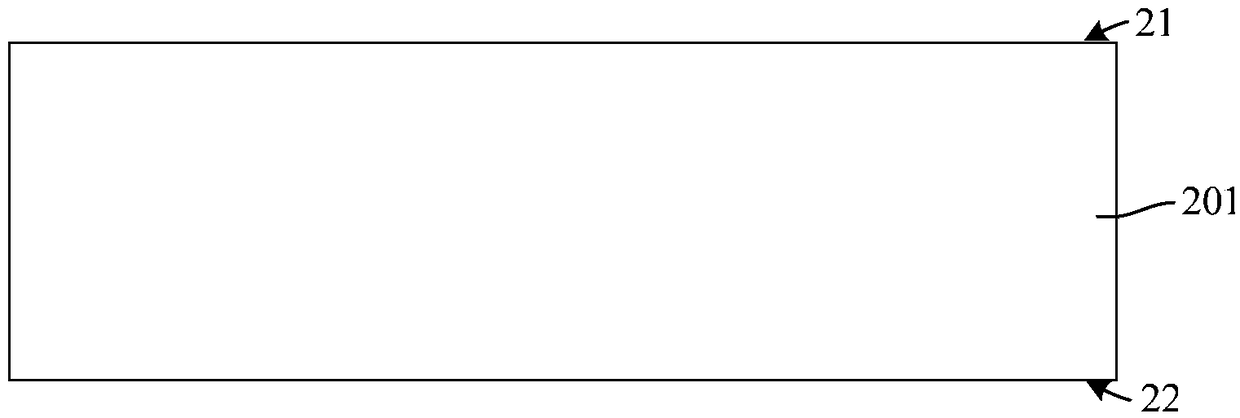
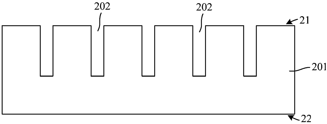
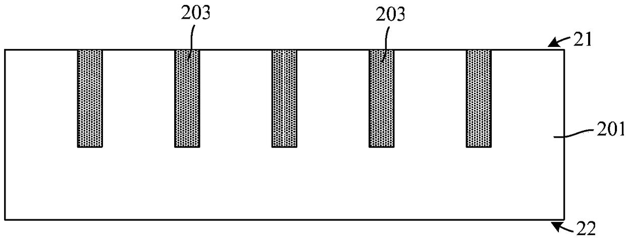
[0029] Therefore, the present invention provides a method for forming a back-illuminated image sensor. In the process of forming the back-illuminated image sensor, no additional epitaxial silicon layer is formed, which reduces the manufacturing cost of the back-illuminated image sensor.

[0030] In order to make the above objects, features and advantages of the present invention more comprehensible, specific embodiments of the present invention will be described in detail below in conjunction with the accompanying drawings. When describing the embodiments of the present invention in detail, for convenience of explanation, the schematic diagrams will not be partially enlarged according to the general scale, and the schematic diagrams are only examples, which shall not limit the protection scope...


PUM


Abstract

A method for forming a back-illuminated image sensor includes: a semiconductor substrate includes a first side and a second side opposite to the first side; Etching the semiconductor substrate on thefirst side to form a plurality of trenches in the semiconductor substrate on the first side; Forming a boron-containing silicon glass layer in the trench, the surface of the boron-containing silicon glass layer being lower than the surface of the semiconductor substrate on the first side; Performing an annealing process to diffuse boron ions in the boron-containing silicon glass layer into a semiconductor substrate between adjacent trenches to form a doping stopping layer; Filling the trench with an isolation material to form a deep trench isolation structure; Forming a pixel of an image sensor on a semiconductor substrate on a first side, the pixel sensing light incident from a second side; Using a doped stop layer and a boron-containing silicon glass layer as a stop layer to thin the semiconductor substrate from a second side of the semiconductor substrate. The doped stop layer and the boron-containing silicon glass layer are removed by wet etching. The above method is simple in process.

Description

technical field [0001] The invention relates to an image sensor, in particular to a method for forming a back-illuminated image sensor. Background technique [0002] Semiconductor image sensors are used to sense radiation such as light. Complementary metal-oxide semiconductor (CMOS) image sensors (CIS) and charge-coupled device (CCD) sensors are widely used in still digital cameras, camera phones, digital video cameras, medical imaging devices (such as gastroscopes), and automotive imaging devices . These devices utilize an array of pixels (which may include photodiodes (photosensitive regions) and transistors) in the substrate to absorb radiation directed at the substrate and convert the sensed radiation into electrical signals. [0003] A backside illuminated (BSI) image sensing device is one type of image sensing device. Backside illuminated (BSI) image sensing devices can be used to detect light from the backside of the substrate. Compared with front-illuminated (FSI...

Claims


Application Information

Patent Timeline
Patent Type & Authority Applications(China)
IPC IPC(8): H01L27/146
CPCH01L27/14689
Inventor 黄心怡王连红
Owner 淮安西德工业设计有限公司
Why Eureka
Try Eureka