Supercharge Your Innovation With Domain-Expert AI Agents!

A polarization conversion device

A technology of polarization conversion and polarization conversion, which is applied in the field of high NA polarization illumination for lithography to achieve the effect of increasing mechanical strength, ensuring stability and ensuring alignment accuracy

Inactive Publication Date: 2017-07-11
INST OF OPTICS & ELECTRONICS - CHINESE ACAD OF SCI
View PDF6 Cites 0 Cited by
  • Summary
  • Abstract
  • Description
  • Claims
  • Application Information

AI Technical Summary

Problems solved by technology

[0004] The technical problem solved by the present invention is: to provide a polarization conversion device, which solves the problem that the light beam is converted from Y polarized light or X polarized light to XY polarized light and YX polarized light in the high NA polarized lighting technology of lithography

Method used


Image

  • A polarization conversion device
  • A polarization conversion device
  • A polarization conversion device

Examples


Embodiment Construction

[0021] In order to better illustrate the purpose and advantages of the present invention, the present invention will be further described below in conjunction with the accompanying drawings and specific embodiments.

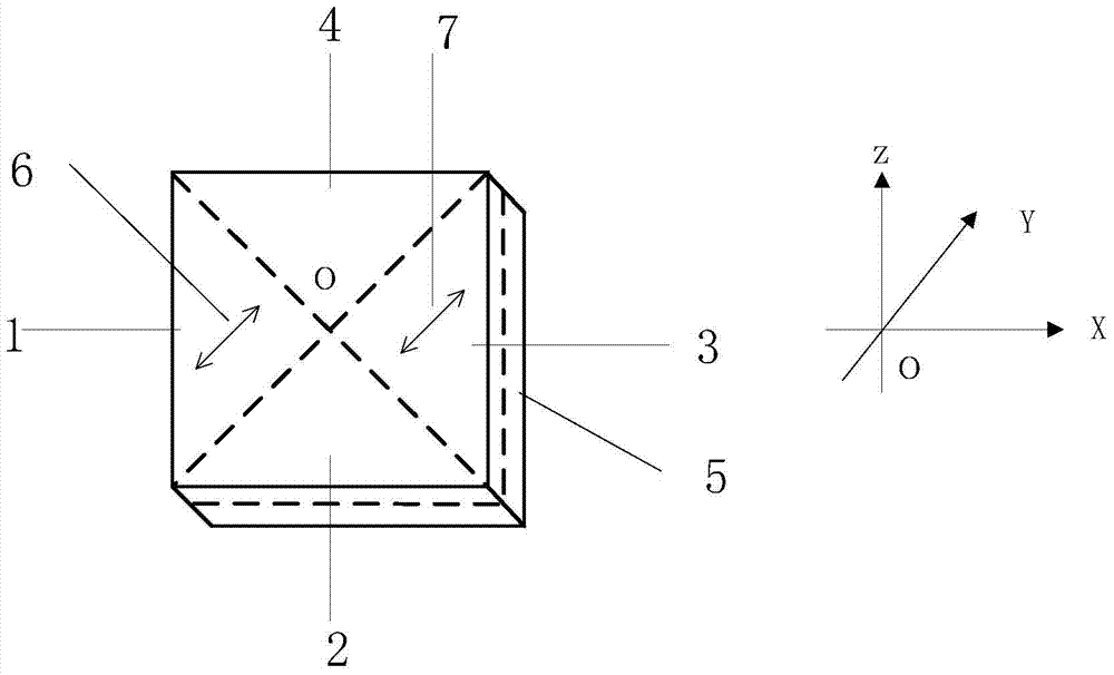
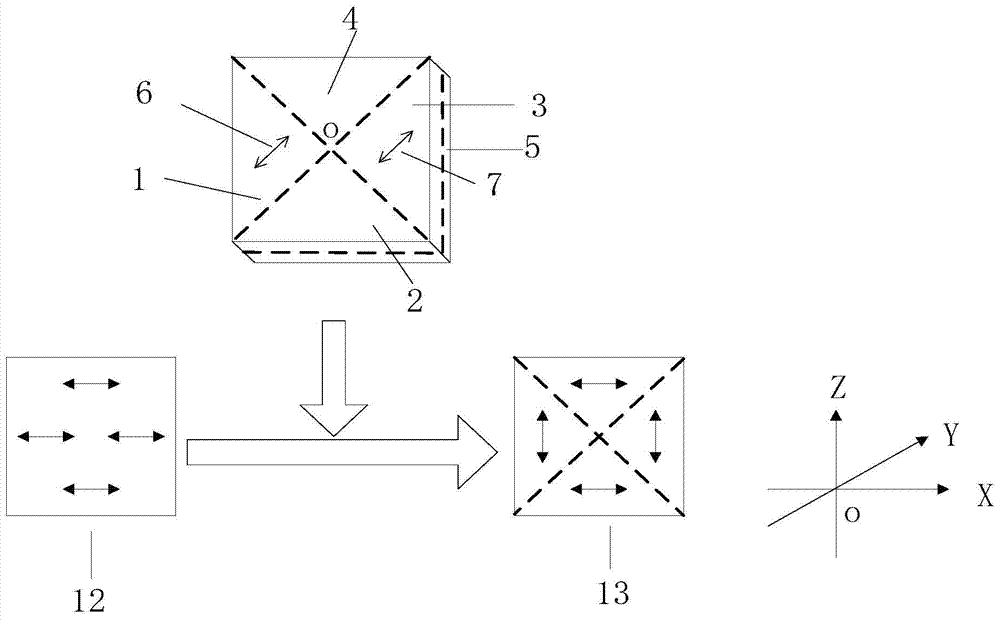
[0022] figure 1 It is a structural schematic diagram of a polarization conversion device, including a half-wave plate 1 , a fused silica substrate 2 , a half-wave plate 3 , a fused silica substrate 4 and a fused silica substrate 5 . Half wave plate 1, fused silica substrate 2, half wave plate 3, and fused silica substrate 4 have central angles of 90 degrees, and half wave plate 1 and half wave plate 3 Arranged alternately with fused silica substrates 2 and fused silica substrates 4, such as figure 1 As shown, the half-wave plate 1 and the half-wave plate 3 have the same thickness as the fused silica substrate 2 and the fused silica substrate 4 and are isosceles right triangles, and the depth optical glue is on the fused silica substrate 5 . The half-wave plate ...


PUM

PropertyMeasurementUnit
angleaaaaaaaaaa
wavelengthaaaaaaaaaa

Abstract

The invention discloses a polarization conversion device, aiming at solving the problems that light beams are converted into XY polarized light and YX polarized light from X polarized light or Y polarized light in the high-NA photolithography technology. The polarization conversion device is formed by two half-wave plates and two fused quartz substrates, which are spliced and deeply cemented on a fused quartz base optically; the central angle of each half-wave plate and the fused quartz substrate is 90 degrees, and the half-wave plate and the fused quartz substrate are the same in thickness; the half-wave plates and the fused quartz substrates are arranged alternatively, the half-wave plates and the fused quartz substrates are spliced into a positive direction, and the direction of the fast axis of the half-wave plate and the X axis form a 45-degree or 135-degree angle. The polarization conversion device has the advantages of good mechanical stability, low processing difficulty, high conversion precision, low cost and the like.

Description

technical field [0001] The invention relates to a polarization conversion device, which belongs to the technical field of photolithography high NA polarization illumination. Background technique [0002] Since the optical projection exposure technology was born in 1978, it has experienced several technological development stages such as g-line, i-line, 248nm, and 193nm. In just a few decades since its appearance, integrated circuits related to optical projection exposure technology have experienced several stages of development, such as small-scale, ultra-large-scale and extremely large-scale, strongly driven by the process of social informatization. Large-scale integrated circuits have become the cornerstone of the development of high-tech fields. From the aerospace fields such as satellites and rockets to the defense fields of radar and laser-guided missiles, as well as various fields of people's daily life, very large-scale integrated circuits are inseparable. It not only...

Claims


Application Information

Patent Timeline
Patent Type & Authority Patents(China)
IPC IPC(8): G02B27/28G03F7/20
CPCG02B27/286G03F7/70008
Inventor 范真节邢廷文林妩媚廖志杰张海波侯梦晗
Owner INST OF OPTICS & ELECTRONICS - CHINESE ACAD OF SCI
Features
  • R&D
  • Intellectual Property
  • Life Sciences
  • Materials
  • Tech Scout
  • Unparalleled Data Quality
  • Higher Quality Content
  • 60% Fewer Hallucinations
Learn More