Array substrate manufacturing method, array substrate and display device

A technology of an array substrate and a manufacturing method, which is applied in the field of display equipment, can solve the problems of high degree of protrusion, pattern disconnection, affecting product yield, etc., and achieves the effect of reducing the disconnection rate and improving the product yield.

Active Publication Date: 2015-07-22
HEFEI XINSHENG OPTOELECTRONICS TECH CO LTD +1
View PDF4 Cites 5 Cited by
  • Summary
  • Abstract
  • Description
  • Claims
  • Application Information

AI Technical Summary

Problems solved by technology

[0004] When the above method is thicker, other patterns (such as source and drain patterns) formed on the overlapping area of ​​the insulating film will have a higher degree of protrusion, and other patterns will easily cause disconnection and affect the product. Yield rate

Method used


Image

  • Array substrate manufacturing method, array substrate and display device
  • Array substrate manufacturing method, array substrate and display device
  • Array substrate manufacturing method, array substrate and display device

Examples


Embodiment Construction

[0079] Reference will now be made in detail to the exemplary embodiments, examples of which are illustrated in the accompanying drawings. When the following description refers to the accompanying drawings, the same numerals in different drawings refer to the same or similar elements unless otherwise indicated. The implementations described in the following exemplary examples do not represent all implementations consistent with the present invention. Rather, they are merely examples of apparatuses and methods consistent with aspects of the invention as recited in the appended claims.

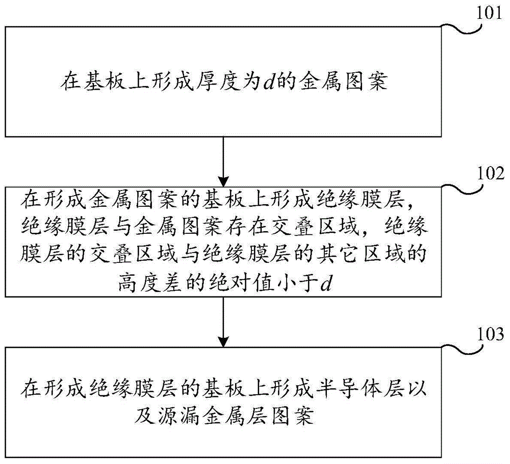
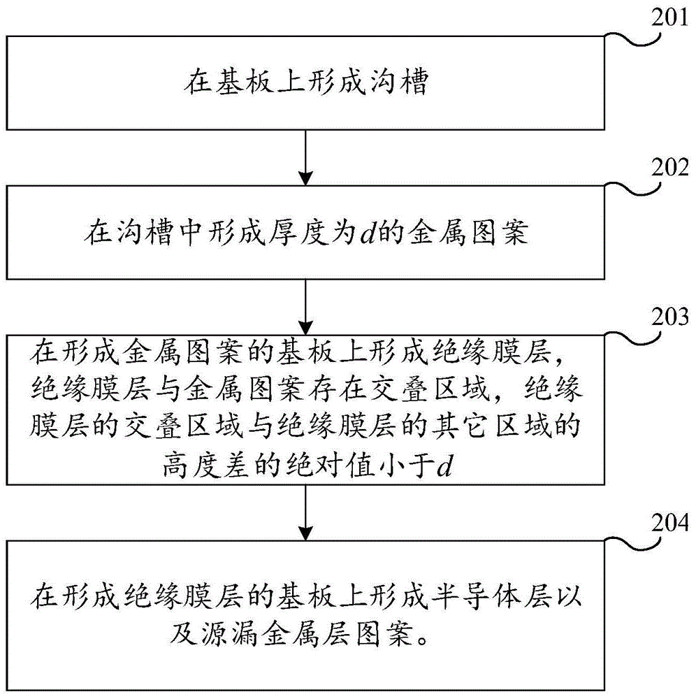
[0080] figure 1 It is a flowchart of a method for manufacturing an array substrate according to an exemplary embodiment. The manufacturing method of the array substrate may include the following steps:

[0081] Step 101, forming a metal pattern with a thickness d on a substrate.

[0082] Exemplarily, the metal pattern is a pattern including a gate line; or, the metal pattern is a pattern incl...


PUM


Abstract

The invention relates to an array substrate manufacturing method, an array substrate and a display device, and belongs to the field of display equipment. The array substrate manufacturing method comprises the following steps of forming a metal pattern with the thickness of (d) on a substrate; forming an insulating film layer on the substrate with the metal pattern; and forming a semiconductor layer and a source and drain metal layer pattern on the substrate with the insulating film layer. The insulating film layer and the metal pattern are overlapped partially, and an absolute value of a height difference between an overlapped region of the insulating film layer and the other region of the insulating film layer is smaller than d. Because the absolute value of the height difference between the overlapped region of the insulating film layer and the other region of the insulating film layer is smaller than d, fluctuation of other patterns formed on the substrate with the insulating film layer is reduced correspondingly, the breakage rate of wires formed on the insulating film layer can be reduced, and the yield of products and be improved.

Description

technical field [0001] The present invention relates to the field of display devices, in particular to a method for manufacturing an array substrate, an array substrate and a display device. Background technique [0002] The array substrate is an important part of the display device, and generally includes the substrate and gate lines on the substrate, common electrode wiring, insulating layers, semiconductor layers, and source-drain metal layers (source-drain electrodes and data lines), etc. [0003] In the prior art, when manufacturing an array substrate, a metal pattern, such as a gate line pattern, is first formed on the substrate, and then an insulating layer is coated on the substrate on which the metal pattern is formed, and then a semiconductor layer and a source are formed on the substrate coated with the insulating layer. Drain the pattern of the metal layer. Wherein, the insulating film layer has an overlapping area of ​​the insulating film layer and the metal pa...

Claims


Application Information

Patent Timeline
Patent Type & Authority Applications(China)
IPC IPC(8): H01L27/12
CPCH01L29/42384H01L29/78603H01L29/78636
Inventor 邹志翔杨成绍黄寅虎
Owner HEFEI XINSHENG OPTOELECTRONICS TECH CO LTD
Why Eureka
Try Eureka